This thread has been locked.

If you have a related question, please click the "Ask a related question" button in the top right corner. The newly created question will be automatically linked to this question.

CCS/LDC1041EVM: Issue with MSP432

Part Number: LDC1041EVM
Other Parts Discussed in Thread: LDC1041

Tool/software: Code Composer Studio

Hi,

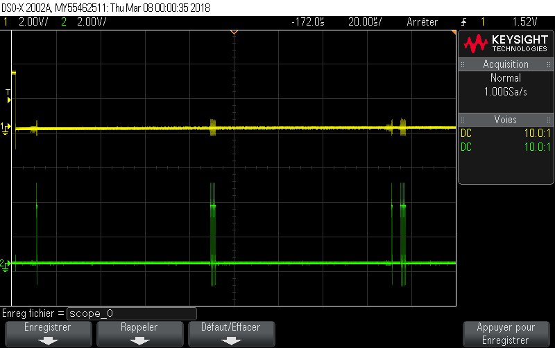
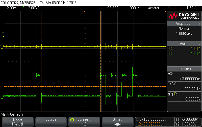
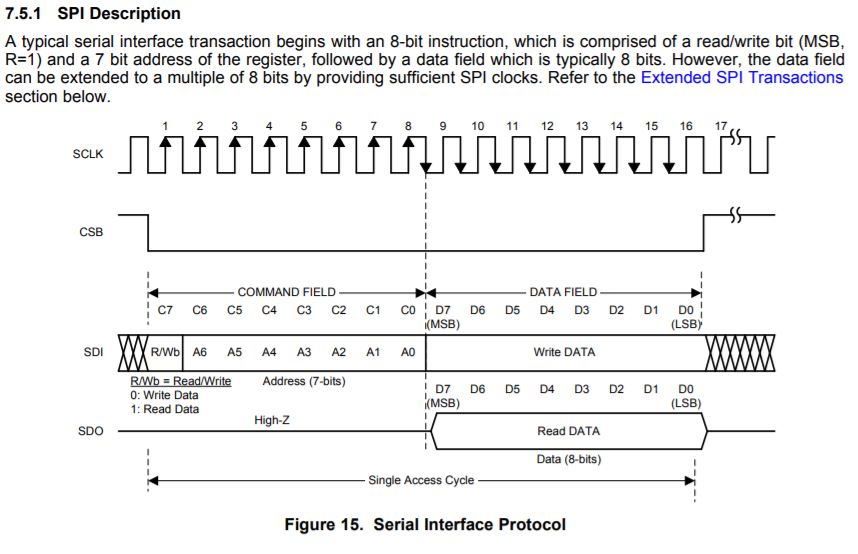
I'm trying to use the LDC1041EVM with a MSP432P401R in register level. I'm facing an issue : I'm trying first just to get the ID of the device (0x84 by defaut). In order to do that, I'm sending 0x80 toward the LDC1041, which corresponds to the code for reading and then the address of the register. I can check on the scope that my asking is right, but I don't have any answer from the LDC1041.

I've tried to program a CSB but it goes down to early : could it be the reason of the problem? Couldn't it just be at the ground at any time?

Another idea is that I don't give any frequency to the LDC1041 on the TBCLK pin, as for the moment I only want the ID. Does the device absolutely needs the frequency in order to work?

Thank you in advance

S.D.

  • Here is my code

    The STE signal seems to appear too early : is there a clock to configure?

    #include "ti/devices/msp432p4xx/inc/msp.h"
    #include <stdint.h>

    uint8_t RXData = 0;
    uint8_t TXData;

    int main(void)
    {
        volatile uint32_t i;
        uint8_t previousData;

        WDT_A->CTL = WDT_A_CTL_PW |             // Stop watchdog timer
                WDT_A_CTL_HOLD;

        P1->OUT &= ~BIT0;
        P1->DIR |= BIT0;                        // Configure P1.0 LED as output

        P1->SEL0 |= BIT4 | BIT5 | BIT6 | BIT7;  // set 4-SPI pin as second function

        EUSCI_B0->CTLW0 |= EUSCI_B_CTLW0_SWRST; // Put state machine in reset

        EUSCI_B0->CTLW0 = EUSCI_B_CTLW0_SWRST | // Remain in reset state
                EUSCI_B_CTLW0_MST |             // SPI master
                EUSCI_B_CTLW0_SYNC |            // Synchronous mode

                EUSCI_B_CTLW0_CKPL |            // Clock polarity high
                EUSCI_B_CTLW0_MSB |             // MSB first
                EUSCI_B_CTLW0_MODE_2 |          // 4-pin mode
                EUSCI_B_CTLW0_STEM |            // STE mode select
                EUSCI_B_CTLW0_SSEL__SMCLK;       // smCLK

        //EUSCI_B0->BRW = 0x01;                   // /2,fBitClock = fBRCLK/(UCBRx+1).
        EUSCI_B0->CTLW0 &= ~EUSCI_B_CTLW0_SWRST;// **Initialize USCI state machine**
        EUSCI_B0->IE |= EUSCI_B_IE_RXIE;        // Enable USCI_B0 RX interrupt
        TXData = 0xA2;                          // Holds TX data

        // Enable global interrupt
        __enable_irq();

        // Enable eUSCIA3 interrupt in NVIC module
        NVIC->ISER[0] = 1 << ((EUSCIB0_IRQn) & 31);


        while(1)
        {
            EUSCI_B0->IFG |= EUSCI_B_IFG_TXIFG; // Clear TXIFG flag
            EUSCI_B0->IE |= EUSCI_B__TXIE;      // Enable TX interrupt
            __no_operation();                    // For debug


        }
    }

    // SPI interrupt service routine
    void EUSCIB0_IRQHandler(void)
    {
        if (EUSCI_B0->IFG & EUSCI_B_IFG_TXIFG)
        {
            // Transmit characters
            EUSCI_B0->TXBUF = TXData;

            // Disable tx interrupt
            EUSCI_B0->IE &= ~EUSCI_B__TXIE;

            // Wait till a character is received
            while (!(EUSCI_B0->IFG & EUSCI_B_IFG_RXIFG));

            // Move data to a temporary buffer
            RXData = EUSCI_B0->RXBUF;

            // Clear the receive interrupt flag
            EUSCI_B0->IFG &= ~EUSCI_B_IFG_RXIFG;

        }
    }

  • Here is another code I tried, but it doesn't work. The goal was to replace the STE signal by a I/O signal

    #include "ti/devices/msp432p4xx/inc/msp.h"
    #include <stdint.h>

    uint8_t RXData = 0;
    uint8_t TXData;

    int main(void)
    {
    volatile uint32_t i;
    uint8_t previousData;

    WDT_A->CTL = WDT_A_CTL_PW | // Stop watchdog timer
    WDT_A_CTL_HOLD;

    P1->OUT &= ~BIT0;
    P1->DIR |= BIT0; // Configure P1.0 LED as output

    P1->SEL0 |= BIT4 | BIT5 | BIT6 | BIT7; // set 4-SPI pin as second function

    EUSCI_B0->CTLW0 |= EUSCI_B_CTLW0_SWRST; // Put state machine in reset

    EUSCI_B0->CTLW0 = EUSCI_B_CTLW0_SWRST | // Remain in reset state
    EUSCI_B_CTLW0_MST | // SPI master
    EUSCI_B_CTLW0_SYNC | // Synchronous mode

    EUSCI_B_CTLW0_CKPL | // Clock polarity high
    EUSCI_B_CTLW0_MSB | // MSB first
    EUSCI_B_CTLW0_SSEL__SMCLK; // smCLK

    //EUSCI_B0->BRW = 0x01; // /2,fBitClock = fBRCLK/(UCBRx+1).
    EUSCI_B0->CTLW0 &= ~EUSCI_B_CTLW0_SWRST;// **Initialize USCI state machine**
    EUSCI_B0->IE |= EUSCI_B_IE_RXIE; // Enable USCI_B0 RX interrupt
    TXData = 0x80; // Holds TX data

    // Enable global interrupt
    __enable_irq();

    // Enable eUSCIA3 interrupt in NVIC module
    NVIC->ISER[0] = 1 << ((EUSCIB0_IRQn) & 31);


    while(1)
    {
    EUSCI_B0->IFG |= EUSCI_B_IFG_TXIFG; // Clear TXIFG flag
    EUSCI_B0->IE |= EUSCI_B__TXIE; // Enable TX interrupt
    __no_operation(); // For debug


    }
    }

    // SPI interrupt service routine
    void EUSCIB0_IRQHandler(void)
    {
    if (EUSCI_B0->IFG & EUSCI_B_IFG_TXIFG)
    {P1->OUT &= ~BIT0;
    // Transmit characters
    EUSCI_B0->TXBUF = TXData;

    // Disable tx interrupt
    EUSCI_B0->IE &= ~EUSCI_B__TXIE;

    // Wait till a character is received
    while (!(EUSCI_B0->IFG & EUSCI_B_IFG_RXIFG));

    // Move data to a temporary buffer
    RXData = EUSCI_B0->RXBUF;

    // Clear the receive interrupt flag
    EUSCI_B0->IFG &= ~EUSCI_B_IFG_RXIFG;
    P1->OUT |= BIT0;

    }
    }
  • Sylvain,
    In the first code example you are sending a different address than in the second. Also, in both cases you continually send the address (either 0xA2 or 0x80). Is this what you intend? Also, should the Chip select that you have picked remain the same state between the address that is transmitted and the data that is received? So, for example the P1.0 should be set low and then the eUSCI buffer loaded with the address and a dummy byte (the transmitter is buffered, so the loads can be back-to-back) and then after the two bytes are received then the P1.0 should be set high.

    Regards,
    Chris
  • Hi Chris,

    Thank you very much for your answer.

    I tried several addresses but no address is working.
    If I understood well the LDC1041, I have to select the chip by setting low the CSB pin during the sending of the address with the read bit, then I let the CSB pin low and wait for a response. In both cases (answer from the LDC or not), I put the CSB pin high back. And I try again (just because it's easier to see the signals on the scope).

    Can the CSB be at low state at any time? Or do I have to put it low at the same time that the clock? The datasheet of the CSB is not clear.

    Thank you

    Sylvain
  • Hello,
    The LDC1041 uses a standard 4-wire SPI protocol. It initiates a SPI read when the CSB transitions from high to low. Then it begins looking for rising clock edges to latch the read/write bit and address bits from SDI on the first 8 rising edges of the SCLK. Assuming the read command was issued (SDI is 1 on the first rising clock edge) the SDO pin will output data from that register on the last 8 falling edges of the SCLK. After your SPI transaction is complete you should pull CSB high. Note, there is a diagram of the CSB, SCLK, and SDI signals in figure 2 of the LDC1041 datasheet as well as a detailed section 7.5.1 SPI Description. I would first confirm with an oscilloscope the signals all look correct and the timing is ok. If your CSB pin is pulled down out of order or after you've been writing to SDI then you will get wrong behavior.
    Regards,
    Luke

  • Hello Luke and thank you for your answer.
    I did all of that. Mu CSB goes low, then I send the read bit, then the seven bit of the address of the register I ant to read. And after that, I let a few time the CSB low in order to let the LDC answer, but I don't have any.
    My question was : is there a time to respect between the falling edge of the CSB and the first clock? My first thought was yes, but I looked at the eval board (MSP430 + LDC1041 + coil) and the time between these two edges is much larger than the one given in the datasheet (in practice it's several µs).

    So what I did is exactly what is written in the diagram given by the datasheet (except for the timing between the fall of CSB and the first clock) at a frequency of 3MHz.
    So, I'm answering, do I have to send a frequency on the TBCLK pin, or can I let it without anything when I only ask for the ID of the LDC?

    Just to be sure, is my code OK? In the second one, I use the P1.0 as the CSB signal. I put it at zero just before the sending of the byte and put it back to high after the receive interrupt (that I never receive).

    Thank you very much for your help

    Sylvain
  • Hello Sylvain,
    Is it possible that you are not meeting the VIH levels of the LDC1041? The VIH is equal to 0.8xVIO, so if you are operating at 5V and have VIO connected to 5V, then VIH level should be >4V. If the MSP430 is operating on a 3.3V supply and has a 3.3V IO, then it would not meet that level.
    To answer the other questions, you do not need TBCLK for SPI communication.
    Regards,
    Luke
  • Hello Luke,

    My analog voltage is 5V, the I/O voltage is 3.3V and the bits I send are 3.18V, so it's more than 0.8*3.3V. Is that okay?

    Thank you

    Sylvain

  • Hello,

    I finally managed to read registers. The program example of the MSP432 was doing everything inside the interruption routine, so I modified the program with flags and now it works.

    I manage to read registers, but I have to send twice the command read. Take a look at the program :

    #include "ti/devices/msp432p4xx/inc/msp.h"

    #include <stdint.h>

    uint8_t RXData = 0;

    uint8_t TXData1;

    uint8_t TXData2;

    uint8_t flag = 0 ;

    uint8_t receive = 0 ;

    uint8_t send = 0 ;

    uint8_t a = 1 ;

    int main(void)

    {

       volatile uint32_t i;

       uint8_t previousData;

       WDT_A->CTL = WDT_A_CTL_PW |             // Stop watchdog timer

               WDT_A_CTL_HOLD;

       P1->OUT &= ~BIT0;

       P1->DIR |= BIT0;                        // Configure P1.0 LED as output

       P1->SEL0 |= BIT4 | BIT5 | BIT6 | BIT7;  // set 4-SPI pin as second function

       TIMER_A0->CCTL[0] = TIMER_A_CCTLN_CCIE; // TACCR0 interrupt enabled

       TIMER_A0->CCR[0] = 2000;

       TIMER_A0->CTL = TIMER_A_CTL_SSEL__SMCLK | // SMCLK, continuous mode

               TIMER_A_CTL_MC__UP;

       TIMER_A1->CCTL[0] = TIMER_A_CCTLN_CCIE; // TACCR0 interrupt enabled

       TIMER_A1->CCR[0] = 1700;

       TIMER_A1->CTL = TIMER_A_CTL_SSEL__SMCLK | // SMCLK, continuous mode

               TIMER_A_CTL_MC__UP;

       EUSCI_B0->CTLW0 |= EUSCI_B_CTLW0_SWRST; // Put state machine in reset

       EUSCI_B0->CTLW0 = EUSCI_B_CTLW0_SWRST | // Remain in reset state

               EUSCI_B_CTLW0_MST |             // SPI master

               EUSCI_B_CTLW0_SYNC |            // Synchronous mode

               EUSCI_B_CTLW0_CKPL |            // Clock polarity high

               EUSCI_B_CTLW0_MSB |             // MSB first

               EUSCI_B_CTLW0_SSEL__SMCLK;       // smCLK

       //EUSCI_B0->BRW = 0x01;                   // /2,fBitClock = fBRCLK/(UCBRx+1).

       EUSCI_B0->CTLW0 &= ~EUSCI_B_CTLW0_SWRST;// **Initialize USCI state machine**

       EUSCI_B0->IE |= EUSCI_B_IE_RXIE;        // Enable USCI_B0 RX interrupt

       TXData1 = 0x01;                          // Holds TX data

       TXData2 = 0x55;

       // Enable global interrupt

       __enable_irq();

       // Enable eUSCIA3 interrupt in NVIC module

       NVIC->ISER[0] = 1 << ((EUSCIB0_IRQn) & 31);

       NVIC->ISER[0] = 1 << ((TA0_0_IRQn) & 31);

       NVIC->ISER[0] = 1 << ((TA1_0_IRQn) & 31);

       while(1)

       {

           if (a==1)

           {

           P1->OUT |= BIT0;

           //TIMER_A0->CTL = TIMER_A_CTL_MC__UP;

           TIMER_A0->CCR[0] = 2000;              // Add Offset to TACCR0

           a=0;

           }

           if (flag==1)

           {

               P1->OUT &= ~BIT0;

               // Transmit characters

               EUSCI_B0->TXBUF = TXData1;

               EUSCI_B0->TXBUF = TXData2;

               TIMER_A1->CCR[0] = 500;              // Add Offset to TACCR0

               flag=0;

           }

           if (receive == 1)

           {

               // Move data to a temporary buffer

               RXData = EUSCI_B0->RXBUF;

               // Clear the receive interrupt flag

               EUSCI_B0->IFG &= ~EUSCI_B_IFG_RXIFG;

               receive = 0 ;

           }

           if (send == 1)

           {

               // Transmit characters

               EUSCI_B0->TXBUF = TXData1;

               EUSCI_B0->TXBUF = TXData2;

               // Disable tx interrupt

               EUSCI_B0->IE &= ~EUSCI_B__TXIE;

               send = 0 ;

           }

       }

    }

    // SPI interrupt service routine

    void EUSCIB0_IRQHandler(void)

    {

       if (EUSCI_B0->IFG & EUSCI_B_IFG_TXIFG)

       {

           // Disable tx interrupt

           EUSCI_B0->IE &= ~EUSCI_B__TXIE;

           send = 1 ;

       }

           // Wait till a character is received

           if (EUSCI_B0->IFG & EUSCI_B_IFG_RXIFG)

           {

               // Clear the receive interrupt flag

               EUSCI_B0->IFG &= ~EUSCI_B_IFG_RXIFG;

               receive = 1 ;

           }

    }

    void TA0_0_IRQHandler(void) {

       flag = 1;

      // TIMER_A0->CTL = TIMER_A_CTL_MC__STOP;

       TIMER_A0->CCTL[0] &= ~TIMER_A_CCTLN_CCIFG;

    }

    void TA1_0_IRQHandler(void) {

       a = 1;

      // TIMER_A0->CTL = TIMER_A_CTL_MC__STOP;

       TIMER_A1->CCTL[0] &= ~TIMER_A_CCTLN_CCIFG;

    }

    I send a first command inside the wwhile(1), and a second inside the interruption routine. If i suppress one or the other, nothing works. Any idea?

    I'm now trying to send two bytes of data : one is the register address, the other is the data I want to write. But as you can see on the pictures below, the two bytes are separated by several µs and I don't know why.

    The yellow trace is the CSB signal. The green trace is the data I want to send. As you can see, the first byte (0x01) is send several µs before the second byte (0x55). Any idea why? I think the two problems are linked : the first one being the impossibility to send a data without writting twice inside the TX buffer and the second one is these two bytes separated.

    Thank you very much for your help

    Sylvain

  • Sylvain,
    I would recommend putting some additional GPIO outputs so you can see the timing of your interrupts relative to when you are sending data.

    Chris
  • Hello,

    Ok I will do that. But have you taken a look to the code? Is there anything that seems wrong?

    Thank you

    Sylvain
  • Hello,

    I tried to use GPIO but I can not see anything interesting, except the fact that from one lign to the next, the program seems to take a lot of time : is there a clock to adjust?

    I don't know why, the principle problem is that I have to send twice the TXBuffer in order to have a response. The response from the LDC1041 is synchronized with the second sent of TXBuffer. So I'm wondering if the answer from the LDC1041 is generated by the clock of the second TXBuffer. In this case, is there something to adjust in the MSP432 registers in order to send 16 clocks instead of the 8 clocks that I send for the moment?

    Thank you for your help,

    Sylvain

  • Sylvain,

    This is what I found in the LDC1041 datasheet on page 15 (  ).

    The SPI transmitter on the MSP432 requires you to write to the TX buffer in order to receive data (generate a clock).  There is no 16-bit mode, so you would need to write to the TX buffer twice, once with the actual address information and then the second write would be a 'dummy' write to receive the data.  In terms of the RX interrupt service routine you will get one interrupt after the address is sent in which the content of the RX buffer is meaningless and then after sending the 'dummy' write another RX interrupt will occur and this time the RX buffer will contain the read data. 

    Regards,

    Chris

  • Thank you very much, all the answers helped me. I'm now able to read and write into registers. The main problem I had was that I didn't pull the CSB HIGH between a write command and a read command.
    In fact, I have to pull the CSB down, to send a first byte with the register address, then the data I want to write. Then I pull the CSB high, then down again and I can send the register address with the 1 at the first bit in order to send the command read, and to finish I send the "dummy" byte and have the data.

    Thanks all

    Sylvain
  • Hi all,

    I need your help again.

    I'm now able to read and write into registers but I have another problem.

    This is a part of the code I'm using to read the LDC1041 :

        TXData1 = 0x0B;                          // Holds TX data
        TXData2 = 0x01;
        TXData3 = 0xA2;                          // Holds TX data
        TXData4 = 0x00;
        TXData5 = 0xA3;                          // Holds TX data
        TXData6 = 0x00;
        // Enable global interrupt
        __enable_irq();

        // Enable eUSCIA3 interrupt in NVIC module
        NVIC->ISER[0] = 1 << ((EUSCIB0_IRQn) & 31);


        while(1)
        {

    if(flag==1)
    {
                P1->OUT &= ~BIT0; // CSB LOW
                // Transmit characters
                EUSCI_B0->TXBUF = TXData1;
                // Transmit characters
                EUSCI_B0->TXBUF = TXData2;
                P1->OUT |= BIT0; // CSB HIGH
    flag=0;
    }


                P1->OUT &= ~BIT0; // CSB LOW
                EUSCI_B0->TXBUF = TXData3;
                // Transmit characters
                EUSCI_B0->TXBUF = TXData4;
                P1->OUT |= BIT0; // CSB HIGH


                P1->OUT &= ~BIT0; // CSB LOW
                EUSCI_B0->TXBUF = TXData5;
                // Transmit characters
                EUSCI_B0->TXBUF = TXData6;
                P1->OUT |= BIT0; // CSB HIGH


        }
    }

    // SPI interrupt service routine
    void EUSCIB0_IRQHandler(void)
    {
        if (EUSCI_B0->IFG & EUSCI_B_IFG_TXIFG)
        {
            // Disable tx interrupt
            EUSCI_B0->IE &= ~EUSCI_B__TXIE;
        }

            // Wait till a character is received
            if (EUSCI_B0->IFG & EUSCI_B_IFG_RXIFG)
            {
                // Clear the receive interrupt flag
                EUSCI_B0->IFG &= ~EUSCI_B_IFG_RXIFG;
                P3->OUT |= BIT2;
                // Move data to a temporary buffer
                RXData = EUSCI_B0->RXBUF;
                // Clear the receive interrupt flag
                EUSCI_B0->IFG &= ~EUSCI_B_IFG_RXIFG;
                receive = 0 ;
                P3->OUT &= ~BIT2;
            }

    }

    As you can see, I send a first byte that puts the LDC into Active Mode, where the conversion is enabled. I use a flag in order to write once only inside this register (at the beginning of the program).

    Then, I send 0xA2 because it is written in the datasheet that data is updated only when a read is initiated on 0x22 register.

    Then I send 0xA3 in order to get the LSB count of the frequency counter.

    But I don't receive any response from the LDC1041, from 0x22 or 0x23 registers. I inject a low frequency (about 10kHz) on the external frequency pin.

    Any idea of something I'm doing wrong? Is there something more to do?

    Thank you for your help

    Regards

    S.

  • Hello Sylvain,
    I would try and use a logic analyzer to better understand how the interrupt service routine is being called. After you load the TX buffer twice, there is one byte in the shift register TXData1 and one byte in the TX buffer TXData2. When the first byte is actually finished transmitting then a receive interrupt will be generated. When the byte TXData2 moves to the shift register the TX IFG is set - but in your case the interrupt is not enabled so it is a don't care. When the TXData2 is transmitted then another receive interrupt is generated.

    In your code flow you have no way to control if the third write to the transmit buffer, TXData3, occurs before or after the TXData1 is sent. It is possible that you are overwriting the data in the transmit buffer. Also, in the interrupt service routine you do not know if you are reading the correct receive byte.

    Another important point is that simply because the transmit buffers have been loaded you should not set the CSB high. The CSB should not be set high until after the data is actually transmitted. This will be indicated by the second RX IFG. Again, you should use a logic analyzer to make sure the program flow and the communication is as expected.

    This example might give you some ideas on how to use sleep and polling to control the flow.
    dev.ti.com/.../

    Regards,
    Chris

  • Hello Chris,

    Thank you for your answer.

    I'm trying the code that you showed me :

    #include "ti/devices/msp432p4xx/inc/msp.h"
    #include <stdint.h>

    static uint8_t RXData = 0 ;
    static uint8_t TXData[20] ;
    uint8_t data = 0 ;

    int main(void)
    {
        volatile uint32_t i;
        uint8_t previousData;

        WDT_A->CTL = WDT_A_CTL_PW |             // Stop watchdog timer
                WDT_A_CTL_HOLD;

        P8->DIR |= BIT0;                        // P8.0 output
        P8->SEL1 |= BIT0;                       // P8.0 option select

        // Configure Timer_A
        TIMER_A1->CCTL[0] = TIMER_A_CCTLN_OUTMOD_4; // CCR0 toggle mode
        TIMER_A1->CCR[0] = 4;
        TIMER_A1->CTL = TIMER_A_CTL_TASSEL_2 |  // SMCLK
                TIMER_A_CTL_MC_3 |              // Up-down mode
                TIMER_A_CTL_CLR;                // clear TAR

        P1->OUT &= ~BIT0;
        P1->DIR |= BIT0;                        // Set P1.0 LED

        P1->SEL0 |= BIT5 | BIT6 | BIT7;         // Set P1.5, P1.6, and P1.7 as
                                                // SPI pins functionality

        EUSCI_B0->CTLW0 |= EUSCI_B_CTLW0_SWRST; // Put eUSCI state machine in reset
        EUSCI_B0->CTLW0 = EUSCI_B_CTLW0_SWRST | // Remain eUSCI state machine in reset
                EUSCI_B_CTLW0_MST |             // Set as SPI master
                EUSCI_B_CTLW0_SYNC |            // Set as synchronous mode
                EUSCI_B_CTLW0_CKPL |            // Set clock polarity high
                EUSCI_B_CTLW0_MSB;              // MSB first

        EUSCI_B0->CTLW0 |= EUSCI_B_CTLW0_SSEL__SMCLK; // ACLK
        EUSCI_B0->BRW = 0x01;                   // /2,fBitClock = fBRCLK/(UCBRx+1).
        EUSCI_B0->CTLW0 &= ~EUSCI_B_CTLW0_SWRST;// Initialize USCI state machine

        TXData[0] = 0x02;                          // Initialize TX data to 0x01
        TXData[1] = 0x3A;
        TXData[2] = 0x03;
        TXData[3] = 0x15;
        TXData[4] = 0x04;
        TXData[5] = 0x17;
        TXData[6] = 0x05;
        TXData[7] = 0x00;
        TXData[8] = 0x07;
        TXData[9] = 0x14;
        TXData[10] = 0x09;
        TXData[11] = 0x12;
        TXData[12] = 0x0A;
        TXData[13] = 0x04;
        TXData[14] = 0x0B;
        TXData[15] = 0x01;
        TXData[16] = 0x22;
        TXData[17] = 0x00;
        TXData[18] = 0x23;
        TXData[19] = 0x00;

        // Enable global interrupt
        __enable_irq();

        // Enable eUSCI_B0 interrupt in NVIC module
        NVIC->ISER[0] = 1 << ((EUSCIB0_IRQn) & 31);

        // Wake up on exit from ISR
        SCB->SCR &= ~SCB_SCR_SLEEPONEXIT_Msk;

        // Ensures SLEEPONEXIT takes effect immediately
        __DSB();

        while(1)
        {
            EUSCI_B0->IFG |= EUSCI_B_IFG_TXIFG;// Clear TXIFG flag
            EUSCI_B0->IE |= EUSCI_B_IE_TXIE;    // Enable TX interrupt
            __sleep();
            __no_operation();                   // For debug,Remain in LPM0


            for (i = 200; i > 0; i--);         // Delay before next transmission
            P1->OUT |= BIT0; // CSB HIGH
        }
    }

    // SPI interrupt service routine
    void EUSCIB0_IRQHandler(void)
    {
        if (EUSCI_B0->IFG & EUSCI_B_IFG_TXIFG)
        {
            P1->OUT &= ~BIT0; // CSB LOW
            EUSCI_B0->TXBUF = TXData[data];           // Transmit characters
            EUSCI_B0->IE &= ~EUSCI_B__TXIE;

            // Wait till a character is received
            while (!(EUSCI_B0->IFG & EUSCI_B_IFG_RXIFG));
            RXData = EUSCI_B0->RXBUF;
            data++;                           // Increment transmit data
            if(data==19) data = 0 ;
            // Clear the receive interrupt flag
            EUSCI_B0->IFG &= ~EUSCI_B_IFG_RXIFG;
        }
    }

    I can check on the scope that my bytes are correctly sent, the CSB is okay and the external clock is oscillating at 190 kHz. But still nothing when I try to get datas from 0x23 register... There is no problem when I get datas from another register. So it seems to me that I forget something important to start the conversion, or maybe a delay that has to be respected?

    Thank you for your help

    Sylvain

  • Sylvain,

       Have you tried to read out the counter using the extended mode?

    Regards,

    Chris

  • Chris,

    I will try but I'm pretty sure it won't work because I don't read anything on the first register 0x22...

    I'm using two power sources : one is the MSP432 itself, which powers the LDC1041 I/O with 3V3 and I use another MSPS432 with the 5V for powering the analog alim of the LDC1041. Is that right?
    Is the external frequency of about 180kHz okay for the LDC1041, or do I have to feed the LDC with a higher frequency?

    Thank you,

    Sylvain

  • Chris,

    Just tried and it doesn't work...


    Sylvain
  • Another thing, when I read the register 0x20, the bit number 6 is always at 1, meaning "no new data available". Does that mean that I don't initiate a measure?
  • Hi,

    I also tried to use the eval board for the injection of the external frequency : I connected the LDCLK clock to the one of the LDC1041 I'm using, and I linked the digital grounds together. It still doesn't work. The only thing I can see is that there is a timing too long between the sending of the bytes 0x22 and 0x23? Is that possible?

    Don't you have a basic code that could read registers 0x22 to 0x25?

    Thank you

    Sylvain

  • Anyone?

    Thank you

    Sylvain

  • Hello Sylvian,

    The expected operation of the LDC1041 requires several items.

    First, the device by default powers into standby (sleep) mode. You must configure the device in this mode, then set the device active by setting the registers. You need to know several things about the sensor, including the minimum sensor frequency and the range of RP of the sensor.

    After setting the device, you can enter active mode by setting register 0x0B to 0x01. You will need to set the CFB capacitor as indicated in section 8.1.3 of the datasheet.

    You then need to wait for completion of the conversion; you can monitor for assertion of the INTB pin if register 0x0A is set to 0x04. After assertion of INTB you can retrieve the conversion data.

    Regards,

    ChrisO

**Attention** This is a public forum