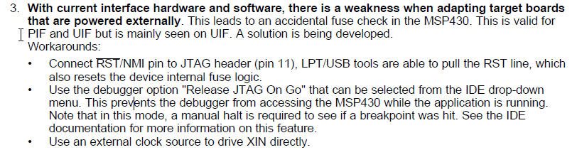
This thread has been locked.

If you have a related question, please click the "Ask a related question" button in the top right corner. The newly created question will be automatically linked to this question.

Microcontroller fries when using external power

Other Parts Discussed in Thread: MSP430F2618

Hello,

I made my own PCB and I am using MSP430F2618. I am facing a problem when powering my device through external power while programming it. I used the configuration given by TI for the JTAG. I connected pin 4 to my VCC rail (3.3V) and left pin 2 floating. Schematic here - https://engineering.purdue.edu/477grp11/docs/pcb_submission/PIT_PCB_LOGIC.pdf .

While powering it through external power, the chip zaps and fries as soon as I put in the JTAG connector. I am powering through a voltage supply so I can see the current draw and it crosses the set limit. I replaced the micro with a new micro on which I put a code which blinks LED. After soldering the micro on the pcb, I power it up using external power, the current draw is 3-5 mA (taken up by the blinking LED) and the code works fine. As soon as I put in JTAG, it fries. Any ideas why? Am I doing anything wrong?

Also, I must tell you that I was able to program it in the beginning 2-3 times before this happened. After replacing the micro, I was again able to program it and then this happened again.

Also, if I try to power my board just using JTAG power (connecting pin 4 to my vcc rail and disconnecting pin 2 from vcc rail), it works fine.

Any ideas why it would do such a behavior with the external power?

Thank You


-Ankit Saboo

  • Hi Ankit,

    Ankit Saboo said:
    I used the configuration given by TI for the JTAG. I connected pin 4 to my VCC rail (3.3V) and left pin 2 floating.

    Ankit Saboo said:

    Also, if I try to power my board just using JTAG power (connecting pin 4 to my vcc rail and disconnecting pin 2 from vcc rail), it works fine.

    isn't this the same?

    So, your schematics says that you're using VCC TARGET (JTAG pin 4) which allows your JTAG to sense the voltage level on your target. Pls correct me if I'm wrong: when you intend to power your target by the JTAG you need to remove 3V3_JMP, disconnect JTAP pin 4 and connect JTAP pin 2 to pin 1 of 3V3_JMP, right? So, looks like your using a custom interface cable? Pls note that the JTAG interface cable lenght must not exceed 8in (20cm) in lenght!

    How many current does your application need? The MSP-FET430UIF can only supply up to 100mA through Pin 2 of the 14-Pin JTAG connector.

    Also, pls notice this Hardware FAQ (http://focus.ti.com/lit/ug/slau278f/slau278f.pdf):

    Kind regards
    aBUGSworstnightmare

  • Hello,

    Thanks for your reply. Yes those two are same, that is my default configuration as shown in the schematic.

    The JTAG headers are soldered onto my pcb. To power the board through JTAG, I just bend the Pin 4 so that it doesnt go in the JTAG connector and short pins 2 and 4. So, this means that pin 2 (and 4) is now connected to my 3.3V rail but since pin 4 is bent down, it is not going inside the JTAG connector. I short pins 2 and 4 using solder as their traces are just next to each other. So, I am using the same JTAG cable which came from TI. My application does not need more than 100mA so the JTAG must be good for that.

    Also, since you asked, I would just mention here that the 3V3JMP was put in place so that I can ensure if the output from the voltage regulator is correct before sending the output to the rest of my circuit. So in case of powering through JTAG, keeping it open or closed won't make a difference as there is no external voltage supply on the other side of the voltage regulator but I still keep it open.

    Thanks for mentioning that there is a problem with the current interface in adapting to externally powered boards. Also, I use the DCO as my clock source, should it be of any concern?


    Thanks Again

    Ankit Saboo

  • The usual suspect here is a ground loop.

    The supply itself has a voltage difference of 3.3V between its GND and VCC. Fine.
    Same for the JTAG programmer. Fine.

    Unfortunately, the JTAGs GND is connected to the USB and therefore to the PC and then to earth. So the programmers GND is possibly different to the supplies GND level, causing a possibly realyl high voltage to appear between the MSP VCC and the programming input pins that fries the chip.

    Ensure that your power supply is galvanically separated from the power outlet, since the PC and therefore the programmer is not.

    And unfortunately, many switching power supplies are not too. The maximum currents are limited by safet capacitors and do no harm to humans, but they often are enough to fry any electronics.

    You can check this by putting a multimeter to the power supply GND and to earth. You'll likely be surprised.

  • Definitely surprised. The voltage difference between them is 12.73 V :|

    But I have a question and it might be a silly one so pardon me. Since I was common grounding them, shouldn't the voltage difference not matter/eventually be the same?

    Thanks Jens-Michael Gross and aBUGsworstnightmare for your help.  I appreciate it.

  • Ankit Saboo said:
    Since I was common grounding them, shouldn't the voltage difference not matter/eventually be the same?

    One should think so, but unfortunately it isn't.
    It may have various reasons, inlcudign wire resistances, inductive potential shifts, cpuling capacitors etc. It is (or at leastr should be) ensured that no current can flow that can harm a human (that is, less than 10mA under any circumstances), but microcontrollers are harmed by the voltage, not the current. The MSP is pretty much protected agains this kind of overvoltages happening on any of its port pins by routign excess voltage to VCC (or GND, if negative), but if its supply itself is affected...

    One example: on some smartphones with touch screen, if the smarthone is connected to the charger adn you touch th screen and then touch someone else (or a grounding pin), you can actually feel that there's something wrong. It's not much and not dangerous to humands, but can be hazardous to electronics.

    One reason for this is the coupling of high and low voltage side of teh power supply to suppress the HF EMI effects of the switched transformer. Usually, a capacitor is used to shortcut these high frequencies from the secondary side back to the primary side of the transformer. Which works well, but has the side-effect that the output is no longer 100% potential free. The capacitor is small, so not much current flows (some µA at max), but it's enough to let some parasitic current flow if you make a second connection to the primary side circuit - by connecting the secondary side's GND to earth, as it implicitely happens when attaching the USB FET through the PC GND and the PC power supply.

    How intense this effect is depends on a wide variety of prameters.
    It is even possible that you see amuch greater or no difference voltage at all if you just rotate the power supply AC plug in the wall outlet (if this is possible - in Germany it is, the plugs are symmetrical) or use a different wall outlet where the phases (line and neutral) are switched

**Attention** This is a public forum