This thread has been locked.

If you have a related question, please click the "Ask a related question" button in the top right corner. The newly created question will be automatically linked to this question.

CCS/MSP430FR6989: Pin Location

Part Number: MSP430FR6989

Tool/software: Code Composer Studio

SO this is a two part question:

Firstly, on the MSP430FR6989 board, where are the P3.4 and P3.5 located? I have looked over the board and could not see the markings anywhere.

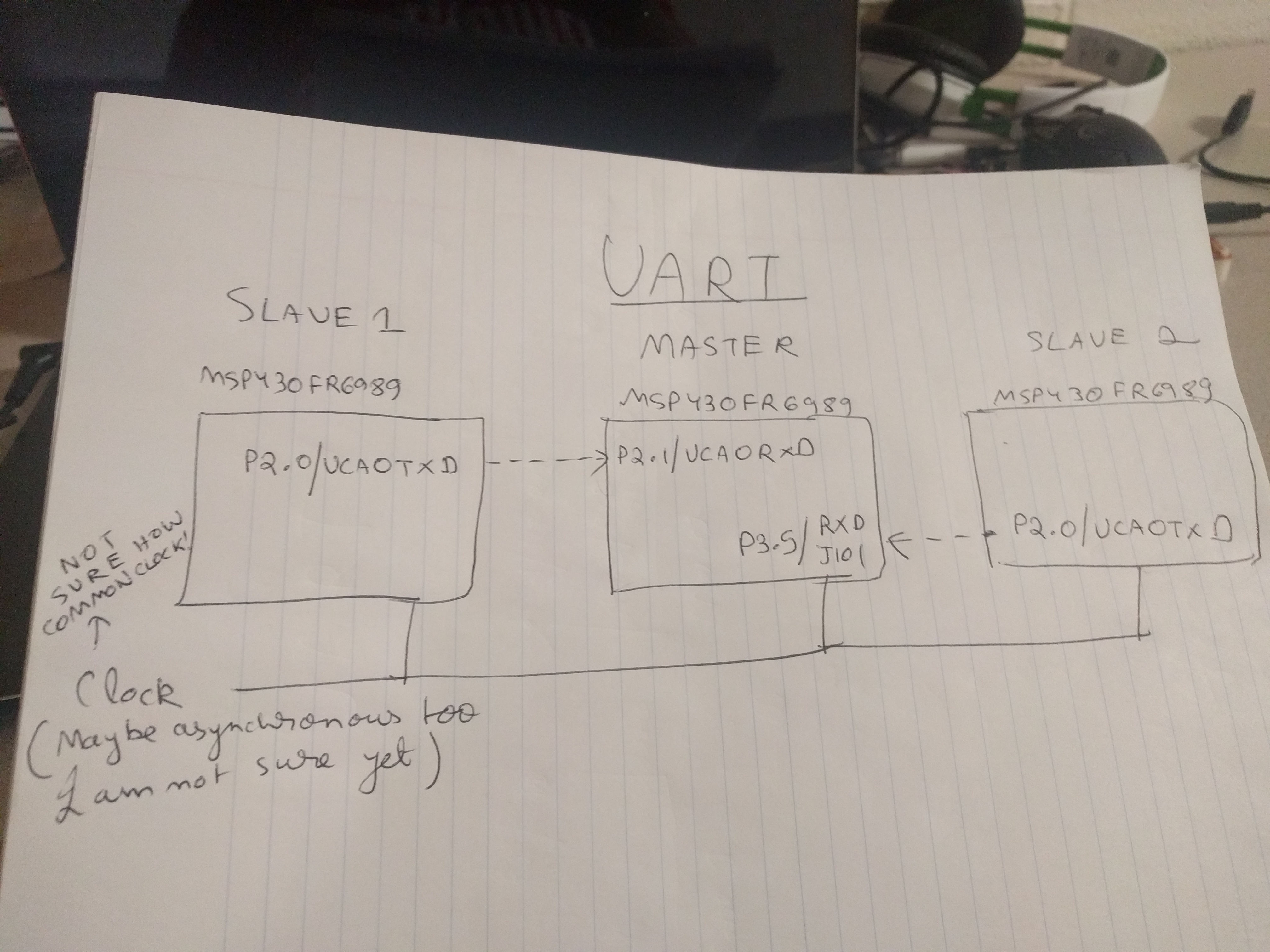
Secondly, is there a good example somewhere on how to set up UART communication in assembler (CCS) between two MSP430s (or one master MSP430 with two slave MSP430s). The example(s) I found in TI Resource Explorer is/are apparently transmitting data to itself and most of the examples online are from MCU to PC.

Thanks in advance. 

  • P3.4 and P3.5 are the TXD and RXD pins on the "bridge" header block (J101), since UCA1 is used for the Backchannel UART. [Ref Launchpad UG (SLAU627A) schematics sheets 1 and 5.] There's no reason you can't pull the jumpers off and connect to them.

    I don't know of any assembly UART examples other than UART_01/_03 in the Examples package (SLAC668G). You should be able to extract code from them suitable to build on.
  • Okay..Why are there two pins for TXD and RXD each? so while making the connections to another board, is it okay if I just use one of the pins?
  • Connect to the MCU side of the bridge. The other side goes over the USB to your PC.
  •  Hmm okay. So, while writing code for two boards, can you tell me how the code is going to be organized. I know in I2C you can choose which pin is master mode and which code is slave mode and each master and slave have their respective .asm/.c files...How do we  achieve the same in UART? Is there going to be multiple asm files?

    What I am really trying to develop is a simple two-person game which will involve three launchpads (two slaves, one for each user) and a single master launchpad, which will simply show the score (on its LCD screen) based off data from the two slave launchpads. The entire game might run up to two-mins max. The game involves inputs from components such as joystick, accelerometer, buzzer, push-buttons (all on BoosterPacks, one attached to each slave).

    So based off my requirements, I have included in the picture at the top what I think I need. I am just not sure how to go about from here.

  • I2C is multidrop, meaning that all the nodes are attached to the same wire(s). Each node, including the master, needs only one port. There is an explicit clock (SCL).

    UART-serial is point-to-point. The Tx and Rx pins are cross-connected (Tx->Rx in each direction) in each link. In your drawing, each slave needs one port (e.g. UCA0) to talk to the master (they don't talk to each other). The master needs two ports (e.g. UCA0 to slave 1 ("left") and UCA1 to slave 2 ("right"). There is no explicit clock, so the nodes' internal clocks have to agree; at suitably low bit-rates this isn't too difficult.

    Using interrupt-driven communication, the master knows which slave an Rx byte came from by which ISR it is executing in. You can only have 2 slaves, since the FR6989 only has 2 UARTs.

    The code for the slaves can probably be identical.
  • Okay based on your instructions, this is what I have for the Master Code and the Slave Codes (which I have included below). For the master code, I was not sure how to implement multiple UART signals so I wrote the code intuitively, setting a UCA1 for every UCA0, assuming they are declared that way. Please let me know if they look reasonable enough or where they should be modified. I based both the code off the UART 3 example for MSP430FR6989 codes in TI Resource Explorer


    ;MASTER CODE UART
    ;MASTER (a MSP430FR6989) CONNECTED TO TWO Slaves (SLAVE_1 and SLAVE_2)
    ;Connections
    
    ;Slave_1 P2.0---->Master P2.1
    ;Slave_1 P2.1 <-----Master P2.0
    ;GND<---->GND
    
    ;Slave_2 P2.0----->Master P3.5
    ;Slave_2 P2.1<------Master P2.4
    ;GND<---->GND
    ;-------------------------------------------------------------------------------
                .cdecls C,LIST,"msp430.h"       ; Include device header file
    ;-------------------------------------------------------------------------------
                .def    RESET                   ; Export program entry-point to
                                                ; make it known to linker.
    ;-------------------------------------------------------------------------------
    RXData1      .set    R5
    RXData2      .set    R7
    TXData      .set    R6
    ;-------------------------------------------------------------------------------
                .global _main
                .global __STACK_END
                .sect   .stack                  ; Make stack linker segment ?known?
    
                .text                           ; Assemble to Flash memory
                .retain                         ; Ensure current section gets linked
                .retainrefs
    
    _main
    RESET       mov.w   #__STACK_END,SP         ; Initialize stackpointer
    StopWDT     mov.w   #WDTPW+WDTHOLD,&WDTCTL  ; Stop watchdog timer
    SetupGPIO
    SetUpP2            
                bis.b   #BIT0+BIT1,&P2SEL0      ; USCI_A0 UART operation
                bic.b   #BIT0+BIT1,&P2SEL1
    SetUpP3
                bis.b   #BIT5+BIT4,&P3SEL0      ; USCI_A0 UART operation
                bic.b   #BIT5+BIT4,&P3SEL1
    UnlockGPIO  bic.w   #LOCKLPM5,&PM5CTL0      ; Disable the GPIO power-on default
                                                ; high-impedance mode to activate
                                                ; previously configured port settings
    
    SetupUART   
                            mov.w   #UCSWRST,&UCA0CTLW0     ; Put eUSCI in reset
                            mov.w  #UCSWRST,&UCA1CTLW0
              
               bis.w   #UCSSEL__SMCLK,&UCA0CTLW0 ; CLK = SMCLK
              bis.w   #UCSSEL__SMCLK,&UCA1CTLW0 ; CLK = SMCLK
    
                mov.b   #8, &UCA0BR0            ; 1000000/115200 = 8.68
                mov.b #8,&UCA1BR0
                bis.w   #0xD600,&UCA0MCTLW      ; 1000000/115200 - INT(1000000/115200)=0.68
                                                ; UCBRSx value = 0xD6 (See UG)
                bis.w #0xD600,&UCA1MCTLW
               
              clr.b   &UCA0BR1
               clr.b &UCA1BR1
                
              bic.b   #UCSWRST,&UCA0CTL1      ; release from reset
             buc.b #UCSWRST,&UCA1CTL1
                
                 bis.w   #UCRXIE,&UCA0IE         ; Enable USCI_A0 RX interrupt
                 bis.w   #UCRXIE,&UCA1IE        ;  Enable USCI_A1 RX interrupt
    
                mov.w   #0,RXData1               ; RXData1 = 0
                mov.w   #0,RXData2               ; RXData1 = 0
    
                mov.w   #1,TXData               ; TXData = 1
    Mainloop    bit.w   #UCTXIFG,&UCA0IFG
                jeq     Mainloop
                mov.w   TXData,&UCA0TXBUF       ; Load data onto buffer
                nop                             ;
                bis.w   #LPM0+GIE,SR            ; Enter LPM0, interrupts enabled
                nop                             ; For debugger
                jmp     Mainloop
    Mainloop2    bit.w   #UCTXIFG,&UCA1IFG
                jeq     Mainloop2
                mov.w   TXData,&UCA1TXBUF       ; Load data onto buffer
                nop                             ;
                bis.w   #LPM0+GIE,SR            ; Enter LPM0, interrupts enabled
                nop                             ; For debugger
                jmp     Mainloop2
    
    
    ;------------------------------------------------------------------------------
    USCI_A0_ISR;    USCI A0 Receive/Transmit Interrupt Service Routine
    ;------------------------------------------------------------------------------
                add.w   &UCA0IV,PC              ; add offset to PC
                reti                                             ; Vector 0: No interrupts
                jmp     Receive                         ; Vector 2: USCI UCRXIFG
                reti                            ; Vector 4: USCI UCTXIFG
                reti                            ; Vector 6: USCI UCSTTIFG
                reti                            ; Vector 8: USCI UCTXCPTIFG
    Receive     mov.w   &UCA0RXBUF,RXData1      ; Read buffer
              ; Do something with RXData1
                bic.w   #LPM0,0(SP)             ; Exit LPM0 on reti
                reti
    TrapCPU     jmp     TrapCPU                 ; Trap CPU
                reti
    ;------------------------------------------------------------------------------
    USCI_A1_ISR;    USCI A1 Receive/Transmit Interrupt Service Routine
    ;------------------------------------------------------------------------------
                add.w   &UCA1IV,PC              ; add offset to PC
                reti                                             ; Vector 0: No interrupts
                jmp     Receive2                         ; Vector 2: USCI UCRXIFG
                reti                            ; Vector 4: USCI UCTXIFG
                reti                            ; Vector 6: USCI UCSTTIFG
                reti                            ; Vector 8: USCI UCTXCPTIFG
    Receive2     mov.w   &UCA1RXBUF,RXData2       ; Read buffer
    ; Do something with the RXData2
                bic.w   #LPM0,0(SP)             ; Exit LPM0 on reti
                reti
    TrapCPU2     jmp     TrapCPU2                 ; Trap CPU
                reti
    
    ;------------------------------------------------------------------------------
    ;           Interrupt Vectors
    ;------------------------------------------------------------------------------
                .sect   ".reset"                ; MSP430 RESET Vector
                .short  RESET                   ;
                .sect   USCI_A0_VECTOR          ; USCI A0 Receive/Transmit Vector
                .short  USCI_A0_ISR
               .sect   USCI_A1_VECTOR          ; USCI A1 Receive/Transmit Vector
                .short  USCI_A1_ISR
                .end
    ; SLAVE_1 CODE
    ;SLAVE AND MASTER ARE TWO SEPERATE MSP430FR6989s...
    ; Connections: 
    ;Slave P2.0--->Master P2.1
    ;Master P2.0 ----> Slave P2.1 (Data received but not used anywhere in slave)
    ;GND<---->GND
    ;-------------------------------------------------------------------------------
                .cdecls C,LIST,"msp430.h"       ; Include device header file
    ;-------------------------------------------------------------------------------
                .def    RESET                   ; Export program entry-point to
                                                ; make it known to linker.
    ;-------------------------------------------------------------------------------
    RXData      .set    R5
    TXData      .set    R6
    ;-------------------------------------------------------------------------------
                .global _main
                .global __STACK_END
                .sect   .stack                  ; Make stack linker segment ?known?
    
                .text                           ; Assemble to Flash memory
                .retain                         ; Ensure current section gets linked
                .retainrefs
    
    _main
    RESET       mov.w   #__STACK_END,SP         ; Initialize stackpointer
    StopWDT     mov.w   #WDTPW+WDTHOLD,&WDTCTL  ; Stop watchdog timer
    SetupGPIO               
                bis.b   #BIT0+BIT1,&P2SEL0      ; USCI_A0 UART operation
                bic.b   #BIT0+BIT1,&P2SEL1
    
    UnlockGPIO  bic.w   #LOCKLPM5,&PM5CTL0      ; Disable the GPIO power-on default
                                                ; high-impedance mode to activate
                                                ; previously configured port settings
    
    SetupUART   mov.w   #UCSWRST,&UCA0CTLW0     ; Put eUSCI in reset
                bis.w   #UCSSEL__SMCLK,&UCA0CTLW0 ; CLK = SMCLK
                mov.b   #8, &UCA0BR0            ; 1000000/115200 = 8.68
                bis.w   #0xD600,&UCA0MCTLW      ; 1000000/115200 - INT(1000000/115200)=0.68
                                                ; UCBRSx value = 0xD6 (See UG)
                clr.b   &UCA0BR1
                bic.b   #UCSWRST,&UCA0CTL1      ; release from reset
                bis.w   #UCRXIE,&UCA0IE         ; Enable USCI_A0 RX interrupt
                mov.w   #0,RXData               ; RXData = 0
                mov.w   #1,TXData               ; TXData = 1
    
    Mainloop    bit.w   #UCTXIFG,&UCA0IFG
                jeq     Mainloop
                mov.w   TXData,&UCA0TXBUF       ; Load data onto buffer
                nop                             ;
                bis.w   #LPM0+GIE,SR            ; Enter LPM0, interrupts enabled
                nop                             ; For debugger
                jmp     Mainloop
    
    ;------------------------------------------------------------------------------
    USCI_A0_ISR;    USCI A0 Receive/Transmit Interrupt Service Routine
    ;------------------------------------------------------------------------------
                add.w   &UCA0IV,PC              ; add offset to PC
                reti                            ; Vector 0: No interrupts
                jmp     Receive                 ; Vector 2: USCI UCRXIFG
                reti                            ; Vector 4: USCI UCTXIFG
                reti                            ; Vector 6: USCI UCSTTIFG
                reti                            ; Vector 8: USCI UCTXCPTIFG
    Receive     mov.w   &UCA0RXBUF,RXData       ; Read buffer
                ; As Slave, do nothing with received data from Master
                bic.w   #LPM0,0(SP)             ; Exit LPM0 on reti
                reti
    TrapCPU     jmp     TrapCPU                 ; Trap CPU
                reti
    ;------------------------------------------------------------------------------
    ;           Interrupt Vectors
    ;------------------------------------------------------------------------------
                .sect   ".reset"                ; MSP430 RESET Vector
                .short  RESET                   ;
                .sect   USCI_A0_VECTOR          ; USCI A0 Receive/Transmit Vector
                .short  USCI_A0_ISR
                .end
    ; SLAVE_2 CODE
    ;SAME CODE AS SLAVE_1 ..CONNECTIONS DIFFER TO/FROM MASTER
    ;SLAVE AND MASTER ARE TWO SEPERATE MSP430FR6989s...
    ; Connections: 
    ;Slave P2.0--->Master P3.5
    ;Master P3.4 ----> Slave P2.1 (Data received but not used anywhere in slave)
    ;GND---->GND
    ;-------------------------------------------------------------------------------
                .cdecls C,LIST,"msp430.h"       ; Include device header file
    ;-------------------------------------------------------------------------------
                .def    RESET                   ; Export program entry-point to
                                                ; make it known to linker.
    ;-------------------------------------------------------------------------------
    RXData      .set    R5
    TXData      .set    R6
    ;-------------------------------------------------------------------------------
                .global _main
                .global __STACK_END
                .sect   .stack                  ; Make stack linker segment ?known?
    
                .text                           ; Assemble to Flash memory
                .retain                         ; Ensure current section gets linked
                .retainrefs
    
    _main
    RESET       mov.w   #__STACK_END,SP         ; Initialize stackpointer
    StopWDT     mov.w   #WDTPW+WDTHOLD,&WDTCTL  ; Stop watchdog timer
    SetupGPIO               
                bis.b   #BIT0+BIT1,&P2SEL0      ; USCI_A0 UART operation
                bic.b   #BIT0+BIT1,&P2SEL1
    
    UnlockGPIO  bic.w   #LOCKLPM5,&PM5CTL0      ; Disable the GPIO power-on default
                                                ; high-impedance mode to activate
                                                ; previously configured port settings
    
    SetupUART   mov.w   #UCSWRST,&UCA0CTLW0     ; Put eUSCI in reset
                bis.w   #UCSSEL__SMCLK,&UCA0CTLW0 ; CLK = SMCLK
                mov.b   #8, &UCA0BR0            ; 1000000/115200 = 8.68
                bis.w   #0xD600,&UCA0MCTLW      ; 1000000/115200 - INT(1000000/115200)=0.68
                                                ; UCBRSx value = 0xD6 (See UG)
                clr.b   &UCA0BR1
                bic.b   #UCSWRST,&UCA0CTL1      ; release from reset
                bis.w   #UCRXIE,&UCA0IE         ; Enable USCI_A0 RX interrupt
                mov.w   #0,RXData               ; RXData = 0
                mov.w   #1,TXData               ; TXData = 1
    
    Mainloop    bit.w   #UCTXIFG,&UCA0IFG
                jeq     Mainloop
                mov.w   TXData,&UCA0TXBUF       ; Load data onto buffer
                nop                             ;
                bis.w   #LPM0+GIE,SR            ; Enter LPM0, interrupts enabled
                nop                             ; For debugger
                jmp     Mainloop
    
    ;------------------------------------------------------------------------------
    USCI_A0_ISR;    USCI A0 Receive/Transmit Interrupt Service Routine
    ;------------------------------------------------------------------------------
                add.w   &UCA0IV,PC              ; add offset to PC
                reti                            ; Vector 0: No interrupts
                jmp     Receive                 ; Vector 2: USCI UCRXIFG
                reti                            ; Vector 4: USCI UCTXIFG
                reti                            ; Vector 6: USCI UCSTTIFG
                reti                            ; Vector 8: USCI UCTXCPTIFG
    Receive     mov.w   &UCA0RXBUF,RXData       ; Read buffer
                ; As Slave, do nothing with received data from Master
                bic.w   #LPM0,0(SP)             ; Exit LPM0 on reti
                reti
    TrapCPU     jmp     TrapCPU                 ; Trap CPU
                reti
    ;------------------------------------------------------------------------------
    ;           Interrupt Vectors
    ;------------------------------------------------------------------------------
                .sect   ".reset"                ; MSP430 RESET Vector
                .short  RESET                   ;
                .sect   USCI_A0_VECTOR          ; USCI A0 Receive/Transmit Vector
                .short  USCI_A0_ISR
                .end
    

  • I haven't reviewed this in detail.

    I'm not too surprised that the UART code is duplicated for the two links. You could build an abstraction for the UART, but that would be a distraction. I suspect you have your work cut out for you just designing the game itself.

    What does this code do when you run it?
  • Till now, I was just trying to establish if using UART was a good idea or not. (if you read the other link, you will probably see all the discussions) I will probably start testing now. The only thing is, would you kindly go over my code for the MASTER? As the MASTER needs two UART channels set up, I am not sure if I have the syntax right or not for doing stuff for eUSCI_A1.

    The game design for the project is almost completed. (atleast the different components of it). Setting up the UART and synchronizing it with the game logic is the last big hurdle.

**Attention** This is a public forum