This thread has been locked.

If you have a related question, please click the "Ask a related question" button in the top right corner. The newly created question will be automatically linked to this question.

TM4C1294KCPDT: SPI terminations for multiple slave

Part Number: TM4C1294KCPDT
Other Parts Discussed in Thread: ADS1298, ISO7840, ISO7841, TM4C1294NCPDT

Hi!

we have a system in which multiple ADS1298 (3pcs) are connected onto the TM4C1294.

The 3pcs ADS1298 are daisy chained together.(with a possibility to Chip select the AFE1, or the AFE2+AFE3 during the initialization/work)

I need a little help regarding the proper termination of the SPI lines(serial termination), especially the SCLK and the MOSI lines (to prevent ringing and to minimize the EMI radiation)

Here is a simplified block diagram.

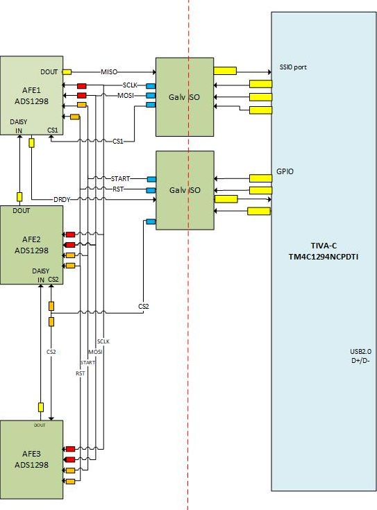
At this point I am sure that the  YELLOW termination points are on good place. But i dont know how is the best to terminate the SCLK and the MOSI line as after the galvanic isolation the lines are routed onto 3 ways, and the 3 section does not have the same lengths. The AFE2 and the AFE3 are close together. 

So my question is where to put the termination resistors ? 

Did i need to put only the at the RED termination points regarding the SCLK, and MOSI, or i need termination also/only at the BLUE points? So to put after the Y split on every leg, or/and before the splitting(too) ?

Same questions i have regarding the other common lines START, RESET, CS, but as these lines wont change their status after the initialization, these lines might not make problems if i put termination only on the BLUE points.

Thanks!

Best Regardss

Lou

  • That is a good question. Of first concern is reflections on the SCLK line. Reflections on this line can cause one or more of the slave devices to see a double clock edge and be out of sync with the master. Slowing the clock frequency will not correct this problem. It is related to rise/fall time of the edges of the clock signal, not the frequency.

    Some basics, the digital signals travel down the traces or wires like a transmission line. Whenever they see a difference in the impedance, it creates a reflection. The path starts with the impedance of the clock source, in your case the galvanic isolator, propagates down the traces and ends at the inputs of the ADS1298s. The first rule is No Y's. The signal should be routed from source to first input, to second input to third input. If it is not possible to route from pin to pin, the stubs must be VERY short. When the clock edge propagates down a trace and sees a Y, it immediately sees half the line impedance and will create a reflection. If it sees a CMOS input on the "side of the road", it sees that as a high impedance in parallel with the line impedance which equates to roughly the same as the line impedance. Therefore, no reflection is created.

    When the clock edge reaches the end of the signal trace at the last input, it sees this as a high impedance and will create a reflection. Here is one correct place to put termination. Three styles of load end termination are "parallel", "Thevenin" and "AC". Unless I am using line drivers that can handle the extra DC load, I use AC load termination. Here is some more information:
    www.diodes.com/.../AB023.pdf

    But since our termination is not perfect, some energy is reflected back to the source where it may see a low impedance and reflect back to the load again. When this second reflection hits the load, that is when we often see an "extra" clock edge. To avoid a reflection back at the source, we can add a series termination resistor to help match the source output impedance to the line impedance.

    OK, what does that mean practically. You need to find the source impedance of the galvanic isolator and estimate the line impedance of your interconnect. Let's assume the galvanic isolator has a source impedance of 50 Ohms, the line impedance is 100 Ohms and you wish to use AC termination. Then you might add a 50 Ohm series resistor right at the output pin of the galvanic isolator. This 50 Ohms added to the 50 Ohms of the galvanic isolator's source impedance then equals the 100 Ohms of line impedance. Then add a 100 Ohm resistor to a 100pF capacitor to ground right at the input pin of the last ADS1298 in the chain. No termination at the midpoint connections to the other two ADS1298s.

    So far I have ignored the MOSI signal. Reflections on this line will not cause an issue, unless they are still present when the slave device is clocked. That means that you can slow down the SPI clock frequency to avoid the reflections corrupting the data. However, if high speed is important, the same techniques can reduce reflections on the MOSI signal.

    A final caution. Adding series termination and AC load termination will slow down the SCLK signal. You may need to balance termination resistor sizes and SCLK speed.
  • *** LIKE *** May I note the "excellence of so thoughtful & caring response" - providing (both) detailed & explanatory guidance - even to include a most helpful "link" to an accessory descriptive source!      Outstanding!

    I would suggest that - in such "difficult to implement pcb layouts/designs" - that (preliminary pcb designs) - focused JUST upon "Iso barrier & SPI devices" be designed, assembled - and then driven/measured/logged & contrasted.     (thus enabling "A-B" circuit comparisons)  

    Along w/"signal reflections" there may exist "standing waves" - which may require additional equipment to detect and to minimize.      Again - impedance "discontinuities" are "prime suspects."     Be sure to include "footprints" for both "termination & series circuit" components - AND (especially) for proper "instrument probe" attachment.     (most always - never/ever properly considered...scope's 3" ground lead FAILS!)

    Thicker pcb traces often help - and often "shorter, more direct trace routings" suddenly "present themselves!"     (due to the designer's/team's "extra time/focus")

  • Hi
    Our SCLK speed is at 12MHz.
    For the galvanic isolation of the MOSI and the SCLK line we are planning to use the ISO7841 isolator, and for the 2nd isolator for other lines (START, RESET, CS) we are planning with the ISO7840.
    Currently im trying to figure out the output impedance of the ISO7841/ISO7840,but i cant found it in the data sheet (we will power them with 3.3V)
    I make a calculation for our microstrip line , it is around 34Ohm for 10mils width.

    I will try to implement the Daisy chain method for the SCLK signal , but it will make longer lines for us if i eliminate the current planned Y splits, and make one long line section -as our source of the SCLK (the output pin of the ISO7841 is about the middle of the 3xADS row).
    Wont this(the long lines) generate delays in the SCLK?So could come to that situation that the clock delays on the last element?
    You also mention that using of series resistance and load termination can cause clock speed issues- slowing down the signal. How can we prevent this? What is important to put lower resistor values/or we can change the line width? Will this make changes in the SCLK speed also?
    Best Regards
    Lou
  • ECGlou said:
    I will try to implement the Daisy chain method for the SCLK signal , but it will make longer lines for us if i eliminate the current planned Y splits, and make one long line section -as our source of the SCLK (the output pin of the ISO7841 is about the middle of the 3xADS row).
    Wont this(the long lines) generate delays in the SCLK?

    The propagation time down a trace is roughly 1.5nS/ft. How long is the trace if it is serial? How long are the two sides if the trace leads from the ISO7841 in two directions?

  • Hi!

    I attached the current status of the design, with the line lengths(total lengths from the ISO output till the SCLK pin on the AFE):

    So Currently there is 1 Y point where the line splits after the ISO onto 2 ways, here are the 2 termination placements, for the 2 leg. But the there is also a split in the section between the AFE2 and AFE3.

    If i make this all from one line than the total length could be 2763mils+4459mils(the distance between the AFE1 SCLK pin and AFE3 SCLK pin)=7222mils of line length form the ISO output pin to the line end.

    Best Regards

    Lou

  • While (outside) poster's interest - would not the placement of the "SPI-based ISO device" - so that any/all SPI signal trace "runs" are minimized - prove a superior method?    "Start, Reset & DRdy" appear "less in need" of trace limitation/optimization.

    The (likely) "Linear Placement" of the 3 ADS devices adds trace length - appears other than well considered - and may likely be IMPROVED...

  • Might I echo cb1's appreciation Bob? Post rises near to tutorial level.

    Robert
  • Ok, if you route SCLK serially, you add about 3.5 inches to the longest trace (7222mils - 2763mils). That increases the delay about 500pS to the delay. At an SCLK frequency of 12MHz, the half cycle time is roughly 41nS. Have you checked the timing of your circuit yet (SCLK out to MISO valid)? If you have the extra time margin for the 500pS delay, (which you should) routing serially can help avoid double clocking due to reflections.
  • Hi
    As we see on our first experimental board,which is similar to the Bob's solution(with SCLK daisy chained), just with shorter wires, as we had at that point different layout - the increasing of the SCLK line wont make us a problem, so its looks like that 500ps delay wont make problem.
    How can i found out the output impedance of the ISO7841? Can i calculate with 20 Ohm?(or i need to calculate the output impedance somehow?)
    Im also looking for this data for the TM4C1294NCPDT.

    Best Regards
    Lou
  • Hi Lou,

    The output impedance of the buffers can be found in the IBIS models. These are text files and there are links to them on the product page. Here is a snapshot from the ISO7841 IBIS file:

    [Pin]  signal_name      model_name           R_pin     L_pin      C_pin         
    1      VCC1             POWER                0.09703   2.25823nH  0.63889pF
    2      GND1             GND                  0.10567   2.15194nH  0.30706pF
    3      INA              IN                   0.12889   1.99554nH  0.21450pF
    4      INB              IN                   0.12623   1.94755nH  0.61276pF
    5      INC              IN                   0.12494   1.92646nH  0.36666pF
    6      OUTD             OUT                  0.14038   2.18765nH  0.43235pF
    7      EN1              EN                   0.17807   2.83638nH  0.45904pF
    8      GND1             GND                  0.08216   2.43955nH  0.44498pF
    9      GND2             GND                  0.10126   2.44074nH  0.40934pF
    10     EN2              EN                   0.17928   2.85707nH  0.52717pF
    11     IND              IN                   0.12883   1.99615nH  0.50841pF
    12     OUTC             OUT                  0.12617   1.94399nH  0.32633pF
    13     OUTB             OUT                  0.12498   1.92454nH  0.37783pF
    14     OUTA             OUT                  0.14050   2.18615nH  0.38097pF
    15     GND2             GND                  0.08275   2.09014nH  0.75096pF
    16     VCC2             POWER                0.09747   2.26909nH  0.67439pF
    

    If I take OUTA (pin 14) as an example, I see it can be modeled as an ideal output buffer to a 0.14 Ohm resistor, then a 0.38pF capacitor to ground, then a 2.2nH inductor then connected to the trace. To figure the output impedance, we need to know at what frequency. It is not the 12MHz of the SCLK signal. Rather we are trying to match the impedance of the reflected edge. From the data sheet, the typical rise/fall time of this signal is about 1nS. Doing a very rough transform, the significant energy is in a frequency with a period four times the rise/fall time, or 1/(4nS) or 250MHz. Now if I calculate the impedance of each element at 250MHz,:

    ZL = 2*pi*freq*L or 3.5 Ohms

    ZC = 1/(2*pi*freq*C) or 1675 Ohms.

    The reflected edge sees 3.5 Ohm  in series with ( 1.6K Ohm || 0.14 Ohm)    (ZL in series with (ZC in parallel with ZR))

    The 1.6K in parallel with 0.14Ohm is basically the same as 0.14 Ohm. Add the 3.5 Ohm and you get 3.64.

    Now, after all of that work, you come to the conclusion that the output impedance of the buffer is so small that I just use a resistor equal to the line impedance. That is true at this rise/fall time. The output impedance calculation becomes more critical with faster switching signals.

    I write like I am an expert in transmission lines, but I really am not. I invite the careful scrutiny of the TM4C community to help provide guidance where I have misled.

  • May I note that your effort is (again) quite good - and while I do have RF/Transmission Line experience - as my past (advising post) met w/silence (other than from poster/friend Robert) - motivation to contribute, "drives to zero."      (some poster diplomacy (simple "thanks" - IS (usually) expected...)

    I will say - again (repeating that past posting) that SO MUCH depends upon the board - its layers (material, thickness, number & overlap) - their relationship - trace widths - and any/all junctions/connections/vias and/or adjacent (especially parallel) traces.     Measurements - also play a helpful role (sometimes "insightful" to the extreme) - (again) I "offered constructive aids there" - also to complete, "poster silence."

    The IBIS file - (essentially) by itself - may not provide the "full & complete picture."     (it is my belief that "most such files" will make that admittance...)

  • CB1,
    Absolutely yes. Calculation of the impedance of the traces on the PCB are not a trivial matter and IBIS models are merely approximations. I do hope that my simple explanation will help the beginning designer understand the concepts of series and load terminations, but I most readily admit that they are just the starting point. As always I appreciate your experienced inputs.
  • Bob,

    Thank you - as I've twice stated (as has friend Robert) - you have gone FAR "Above/Beyond" the "normal/customary" vendor (time-driven) response w/this poster.        And - dare I say - very much of this thread's content, "Veers far from its (rather narrow) MCU-centric Lane!"     (our move from Power/Cordless Tools to Autonomous Auto (induces) "roadway & sudden, unwanted, heading-shift" jargon - sorry...)

    The importance of this subject (and similar) greatly (and necessarily) magnifies - when one is tasked w/controlling (multiple) BLDC Motors - each drawing > 100A RMS - from (each) of the motor's 3 Phases.    Under these conditions - very accurate "Impedance Measurements - and (proper) impedance matching" - even when - and especially when - the motor load, speed, and (both) motor & Power FETs' temperature make (very) wide excursions - proves great challenge.      (likely exceeding that here - yet offering (profound) insight & focus...)

    As one example of such "insight/focus" - our group typically will restrict the "initial" pcb design to, "Just the devices of interest!"      And then - after exhaustive, "test/measurement" (and data logging) produce "best considered"alterations to that base design - in the "hope" that such (real world, "A-B comparative data) will, "Point the way towards layout optimization!"      Note that these (necessarily) smaller boards are, "Faster, Easier and Less Costly" to design/develop & assemble/populate - then test!     And - they (very well) meet the directives of, "KISS!"     In contrast - the (usual) "whole board designs" - restrict, hamper & generally impede such (necessary) "Search for Optimization!"      (while being more labor intensive & more costly!)

    Firm/I engage top Univ. Professors, Industry Experts, Most Modern/Focused (i.e. expensive) Test Equipment - and STILL - multiple (KISS-Based) board implementations ARE - without doubt - DEMANDED!     I suggested such (iterative based approach) because the "best/brightest - most focused" - have "Found that to be mandatory!" 

    Certain of our "Aero/Defense" work involves board materials/capabilities (even methods) which prove "far beyond" - that (normally) found here.      And - even w/such "quality, attention, & expertise" - the "Iterative, Carefully Considered - only then Implemented & Measured, "KISS-Based, Single-Step Process" remains REQUIRED to, "Speed, Ease & Enhance" Pcb Implementation Success.

    Is it not said that, "All roads (lead to) Rome?"       And - perhaps equally - all challenging - yet (near) optimal Pcb Layout Implementations (stem from) "KISS."

  • Dear cb1_mobile,Bob!
    I appreciate the help and the information i got from you both!
    Unfortunately i don't have too much experience in the transmission lines technics.
    I dont expect that you will solve my problem, neither i want to get a final solution from you, i just need to get some signpost on this road, and on what i have to watch.

    At this point we dont have a time frame/budget to make one more testing circuit, so on the next board i want to do the things as good as it can.
    We found a lot of mistakes, and at this point only the SPI line matching is left what we think was a potential EMI problem source(we hope we eliminate all other EMI sources with a correct layer stack and with a ground/power plane redesign-without gaps)
    I will put those spots inside the line for termination as you cb1_mobile mention, at this point my goal was to tune them as much closer to the final value. I know and understood that this is not a simple calculation, and there are too many variables to give at this point a final answer, i only wanted to understood how it should be done.

    Best Regards
    Lou
  • Thank you - far better to receive (some) response (even a belated one) than (dismissive) "silence."       (few here, "rise to your aid" - silent dispatch FAILS!)

    Not having, "Time-frame/budget" to produce the suggested, "highly focused, multiple (guiding/probing/learning) board iterations" - proves a "most common & destructive shortfall" - to so many!       Minus such intense/limited pcb design focus - how can you (ever) "really know" the impact and contribution of your "multi-device, SPI-based, design elements" upon your board's overall performance - and "unwanted" offensive signal generation?    (both radiated & conducted!)       W/in the medical/surgical theater - is not the (area of specific interest) "draped" - so as to insure, "KISS-based, Complete & unfettered FOCUS?"

    What is your/firm's LOSS - should the (focused - (i.e. "iterative - proceed by refinement") effort (which you've rejected) results in, "Regulatory Agency test failure?")      What then?

    KISS has long existed for (very) good reason - it is believed that the, "case for its implementation" has been "reasonably" presented...    (even with - especially with - (claimed) time/budget constraint!)