This thread has been locked.

If you have a related question, please click the "Ask a related question" button in the top right corner. The newly created question will be automatically linked to this question.

TM4C1299KCZAD: ULPI Interface Timing Diagram

Part Number: TM4C1299KCZAD

Dear Champs,

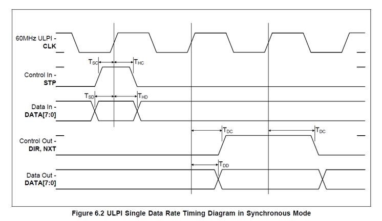
As we check ULPI Interface Timing Diagram in datasheet, we saw below figure:

But it seems have some different with ULPI spec.

And it's also different with Microchip high speed PHY, USB3220C.

Why our ULPI signal need delay U5 when clock rising up? Rather than start up TSC time before clock rising up? 

If you have any suggestion, please feel free to let me know.

Thanks a lot.

Best regards,

Janet

  • Hi Janet,
    We are looking into this. We think it is just a wrong diagram and timing U5 should be referenced from the falling edge, not the rising edge.
  • Dear Bob,

    Will it affect high speed USB PHY working?

    In my understanding, if host identify the USB com port, the timing of USB is correct.

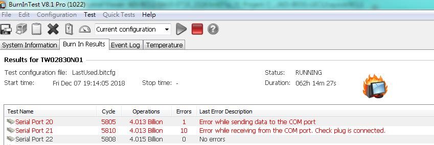
    See below two error messages when testing USB Burnin progress.

    If we meet error of byte 0 or TX/RX package, does timing of USB affect this? 

    If you have any problem, please feel free to let me know.

    Thanks a lot.

  • Hello Janet,

    Sorry for the delay on this, I was reviewing ULPI specifications and a few other resources to be able to properly explain the diagram.

    I will clarify/answer two separate parts of the original question.

    Part 1: ULPI Timing Diagram looks different from specifications

    The official ULPI documentation actually has an image that represents the STP in the same way as we do on our datasheet but without the timings included, see Page 12: www.sparkfun.com/.../ULPI_v1_1.pdf

    This same document on Page 21 has the timing diagram you shared.

    So we just used that first image on Page 12 as the basis for our diagram rather than the second image. Probably have used the second one as it's better for showing timings, but in any case the diagram is correct unlike our initial thoughts due to how the clock was represented.

    Part 2: Why does U5 show a Delay and not a hold/setup time for STP signal?

    The ULPI documentation is a little poor here in the sense that it implies both sides would look the same, but in reality we are looking at a diagram with shows both inputs and outputs, and it only shows it from the PHY side.

    In other words, the STP signal in that diagram is an input, and the DIR/NXT signal is an output.

    Based on this, they showed the timing spec for inputs and outputs.

    What that representation does not reflect is that the MCU is the inverse of this. In other words, the STP signal is an OUTPUT for the MCU and the DIR/NXT signal is an INPUT.

    Therefore, for the MCU, STP falls under the "control out" specs, and has to have a delay time. This is what is shown with U5.

    Meanwhile, DIR/NXT is the "control in" and the specs for that require a setup time and a hold time which are shown with U1/U3.

    Therefore the timing diagrams for the device are accurate in their portrayal of these signals.