This thread has been locked.

If you have a related question, please click the "Ask a related question" button in the top right corner. The newly created question will be automatically linked to this question.

Non Volatile Memory Lifetime / Endurance

Other Parts Discussed in Thread: TM4C1294NCPDT

A couple of very basic questions about non-volatile memories lifetime / endurance:

- Does READING eeprom have any impact on its lifetime? Or is it safe to read it a gazillion times, with the 500,000 limit just for WRITE operations?

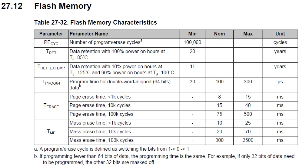
- For WRITE CYCLES, does the FLASH memory have any sort of similar life limitation on TM4C devices such as EEPROM has?

Context: currently working to improve some features of our products, and trying to organize where/how to store a few "status and configuration" parameters that can change from time to time... Let's say one can be concerned that the product will fail after 1370 years if these parameters are rewritten to eeprom once a day...

  • EE and Flash do not have read wear out mechanisms that I'm aware of. They do, however, have a finite lifetime. If you check the data sheet you'll see a data retention time specified. As I recall it's 20 years.

    If you need a large number of write cycles then the memory of choice is FRAM (Maybe MRAM but I've not seen much selection available).

    Oh, and if using EE or FLASH on chip, check the errata.

    Robert
  • Thanks Robert!
    My original second question was not clear as I read it again, so I fixed it. On flash memories, does the write limit also apply?
    And now that you mention, I am aware of the MSP430 with FRAM, but are there already/planned TM4C's available with such?
  • Hello Bruno,

    There are no TM4C parts available with FRAM. As of now, there are no planned devices with FRAM.

    The following is a "Flash Memory Characteristics" table for the TM4C1294NCPDT device. Please verify the datasheet for the device you are interested in.

    Thanks,

    Sai

  • Actually, I was thinking of an external NVRAM when I mentioned FRAM. Also avoids the errata I mentioned earlier.

    Robert
  • Thank you all,
    Yes, I was referring to internal NV memories on both cases.
    Interesting that I had missed flash memory erase cycles information on the datasheet... I was "sure" of that implication of flash memories, but I was looking elsewhere on the document and missed such table.
    My "best practices notes" will remain: neither flash nor eeprom are eternal. If you need to store non volatile parameters, update them "with care", really only when needed - and among the two options, prefer eeprom. If the amount of rewrite cycles tend to be high, invest on a FRAM external IC (and benefit from the also typically lower power for writing!)
    Cheers,
    Bruno
  • Hello Bruno,

    As Robert pointed out, please refer the errata for both TM4C devices before making a decision of going with EEPROM.

    Thanks,
    Sai
  • Errata dully read...
    It almost states "do not use eeprom"!
    A bit of focused programming work can try to guarantee that eeprom is not written when dma is running, and can isolate eeprom calls from possible software resets as suggested on the errata.
    But it is really hard to tell end user to "avoid pulling the plug out" during those exact miliseconds in which my stupid code decided to modify the eeprom... Well, I guess that, unless the application involves life risk or a mission to Mars, it is a really rare possibility that most products can live with.

    It reminds me of an old idea... at the waste of a GPIO, maybe uC's should have some "about to run out of power" state, and some sort of backup power supply pin connected to a slightly bigger cap. When the "about to run out of power" gets detected, an interrupt brings code execution to an application which "saves whatever needs saved". Well, it's too specific, and can already be designed using external circuitry... so never mind, still I'll just leave the concept here.
  • Bruno Saraiva said:
    If the amount of rewrite cycles tend to be high, invest on a FRAM external IC (and benefit from the also typically lower power for writing!)

    They are also much faster which makes them simpler to program because

    1. you don't have to check for write complete
    2. If a power down can occur during programming and you need to ensure the write completes the hold up supply can be much smaller

    Robert

  • NAND FLASH suffers from an effect called read disturb, where repetitively reading an area of memory can affect adjacent cells. Most microcontrollers, however, use NOR FLASH rather than NAND, so are not susceptible to read disturb,

    Some microcontrollers with "EEPROM" actually have the EEPROM implemented as FLASH with some logic wrapping it. I don't know if the Tiva 4C implements its EEPROM this way, however.

  • Bruno Saraiva said:
    It reminds me of an old idea... at the waste of a GPIO, maybe uC's should have some "about to run out of power" state, and some sort of backup power supply pin connected to a slightly bigger cap. When the "about to run out of power" gets detected, an interrupt brings code execution to an application which "saves whatever needs saved". Well, it's too specific, and can already be designed using external circuitry... so never mind, still I'll just leave the concept here.

    I've done that before.  It doesn't actually need to be an interrupt (probably better if not).  Just poll before writing and set the pin such that if there is not sufficient power to complete the write (with generous margin) then the write is not started.

    One of the problems with the TI EE implementation is the extremely long worst case write scenario, it runs to seconds.

    Robert

  • TI does implement the EE in FLASH. It's rather obvious when you read the specs and there are some definite side effects of it doing so.

    I didn't know that about NOR, thanks for that.

    Robert
  • "I didn't know that about NOR" - nor did I - thank you * 2...

    Might this be an issue endemic to all such devices - or limited to certain makers?

  • Bruno, there are a couple of more down to earth scenarios besides life support that would lead to being wary of such corner cases.

    For instance there is the case where replacing the board requires a flight to a remote area, or where a production line is stopped until the board is replaced.

    Robert
  • To add some comment to the original post/question:

    While Flash/EEPROM does not have a "read wear-out", the life time of the programmed data (state) is limited. This is caused by the isolated gate technology itself. Programming means to tunnel electrons via higher voltages onto the isolated gate, that stay trapped there. Cosmic radiation or similar effects will "free" this charges over time (call it entropy). That is the reason for the "data retention time" which vendors of those ICs specify in the datasheets, usually in the range of 10 years. Placing your device in high altitude, in space, or at elevated temperature will decrease data retention - the data are just "gone", while the EEPROM/Flash still functions well.

  • Much data of interest here - thank you f.m.

    Might aggressive EMI shielding - ranging from conductive coatings w/in a plastic enclosure and/or more intense metal shielding serve as a defense mechanism?

    It would appear that one (non-shielding) defense would be to copy such data into "fresh cells" - not so often as to invoke flash "wear-out" - yet sufficiently to avoid the "freeing of charge."  

    In addition - I wonder if the (rare but rising) "limited corruption of our MCU's flash" (from several ARM vendors) may result from locating our MCU too close to our 1KW BLDC motors.   (equipped w/powerful, top-grade, "rare-earth" magnets - and motor spun up to 22K RPM)

    Might you comment?    Thank you...

    Students' (long standard) excuse of, "Dog ate my homework" may (now) have a "techier" excuse, "Cosmic radiation."    (more modern, "perp!")

  • I agree with you all and appreciate when a thread becomes more of an engineering/development platform!

    Last evening I was thinking of a sort of "circular anti-aging" memory allocation just as suggested by CB1. But either the index must be stored somewhere (which might as well fail), or maybe have the address dynamically calculated, for example, from GNSS acquired real time - subject to errors and hell of a complex, expensive solution...

    Comments with no expertise at all: I'll continue to rely on the embedded eeprom only when the failure doesn't risk lives, a halted production line or a long trip to a remote locations (I like remote locations, and if whoever has to pay for it refused to invest on a better memory solution up front, then I'll go at someone else's expense!)

    Anyway, FRAM's would probably be the choice. I do have a FRAM chip on a few of the previous projects, and will get back to them in the near future as I'll have to make an ultra low power device which will require a "relatively good amount of memory". That one ain't going to space (non of them do...), so I'll stay clear from the mechanical shielding.

  • Bruno Saraiva said:
    That one ain't going to space

    Neither do (most) of ours - at least, "Not on purpose."   (our lab's ceiling serves a 2nd role as vertical buffer for "launched" components)

    Yet - long ago - we produced a small, "Command/Control" module w/display & soft-keys - which flew (successfully) twice on the Shuttle.   We struggled to apply conductive coating to our custom plastic enclosure (and that worked) yet U. of Alabama @ Huntsville (prime NASA contractor) failed our plastic due to, "out-gassing."   They then machined enclosures from aircraft-grade aluminum - so thin that they were remarkably light - and that approach met, "radiation, out-gassing & weight" requirements...

    Your agreement to, "travel anywhere - so long as the (other guy) pays" - may require a, "mileage and/or altitude" escape clause...   (which I can draft - & "Luis" can translate)

  • In addition - I wonder if the (rare but rising) "limited corruption of our MCU's flash" (from several ARM vendors) may result from locating our MCU too close to our 1KW BLDC motors.   (equipped w/powerful, top-grade, "rare-earth" magnets - and motor spun up to 22K RPM)

    I'm not really an expert in this ground-level IC physics, just remembering what I picked up on the way. However, I suspect that your apprehension is justified. The reduction of structural sizes and technological improvements of increase bit density definitely have the "side effect" of reducing robustness towards energetic influences (particles and fields). A Renesas FAE told me a few years ago, with structure sizes less than 100 nanometers, the implementation of ECC for SRAM (e.g. in MCUs) is imperative. Else the bit errors would crash the code in a matter of seconds or minutes.

    Another observation - if two (or more) companies list their ICs as of the same class (i.e. "FLASH"), it doesn't mean they use the same or even similar technology. And obviously, Flash technology is seen as trade secret and advantage over competitors. That would explain large differences in "waitstate-less" operation ranging from 25MHz to 100MHz for otherwise equivalent MCUs.

    As further reading and starting point, I would suggest https://en.wikipedia.org/wiki/Charge_trap_flash

  • I did comment, but included a link that probably looked "suspicious" and needs moderation.
    So perhaps it gets eaten by the forum...

    Edit: the TI forum moderator seems rather quick !!!   ;-)

  • I've found that external links trigger moderation most if not all of the time.

    Robert
  • Similar to f.m. It's been years since I was studying in the area and that was non-device work.

    However, as a few notes. Other things being equal smaller structures are easier for carriers to tunnel through so there is an enhanced leakage from size reductions. Electric fields will increase tunneling probability so another increased leakage. Charged particle radiation ionizes the barrier. The last used to be a big problem in DRAM even decades ago due to radiation from the packaging material. I understand that to have been much reduced but maybe as the geometry has been shrunk the probabilities have started to rise again. It's possible magnetic fields could affect tunneling probabilities but I don't know of a mechanism which is probably just a gauge of the depth of my ignorance.

    Also as the voltage is lowered the sensitivity to noise increases decreasing the margin for detection of bit state.

    Robert
  • If - or if not - directed towards moi - merci to (both) posters f.m. & Robert.

    Our ten year older, giant when compared, "Franken-MCUs" appear "Far more resistive" to such, "radiation, charge & fields" than the new, "latest/greatest." (this in direct support of the theory you've both presented...)

    (this via "A-B" MCU comparison - "new appears (not always) entirely, better!"