This thread has been locked.

If you have a related question, please click the "Ask a related question" button in the top right corner. The newly created question will be automatically linked to this question.

JTAG - TDO is constant high


Hi all,

There is another question in the forum with a similar title, but the solution for that problem is not my case, so here we go again.

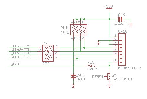
Using IAR, fully updated. The board is a custom project, in which the JTAG is the same as we have been using for other ARM TM4C projects successfully. The JTAG diagram is attached. Do not mind the different picoblade 8-pin connector, as I am triple sure that all pins are where they should go.

The same IAR workbench and project compiles and uploads properly with another board that we have. The problem is hidden somewhere in this new board. We assembled two boards, and both have the exact same result. I supected a bad IC, and replaced the TM4C123AH6PMI chip from one of them, same problem.

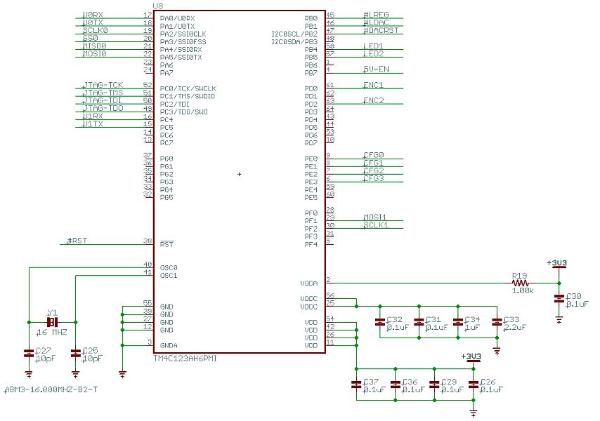
The schematics below is the IC part of the board. I checked each 3V3 pin, they are all good (3.24V), each ground pin, they are properly grounded, and the VDDC pins are also coherent (1.095V)

First question: is this the typical signal expected on TDO when the JTAG pin is NOT connected? It is high at 3.24V, with spikes coming down to about 1.7V at 135Hz. With JTAG connected, the shape is similar, but it goes down to approximately 2.5V. Image below:

I have a couple more brand new sample IC's here, from a different shipment, but I am avoiding to replace an IC again, because the first time I did it the result was exactly the same, so maybe someone out there can give me another hint - resoldering IC's are painful for the board...

What else has been checked:
- The pull up resistors are confirmed to be 10K. Measured twice, and replaced twice. No shorts between any of them.
- The 27R resistors are confirmed to be 27R. I even removed them and connected the pads directly to have no resistance. The resistance was confirmed all the way from the IC pins to the JTAG 14-pin header.
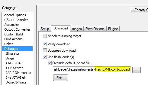
- Tried to change the connection option on IAR's J-Link settings from JTAG to SWD, no results.

Thanks in advance for the help! 

  • This is becoming a nightmare... I decided to replace the uC, with a brand new one just received from TI.

    Exactly the same result: no JTAG communication. Again, tested all the 3V3 pins, all the VDDC pins, grounds, IO's, all seem to be fine.

    I also read elsewhere that the power up can be particularly critical, this is a scope view of the power up voltage.

    I must be forgetting some really stupid detail, I can't assume that three uC's were shipped faulty, from three different shipments...

  • Feel your pain - loss of JTAG always unsettling.

    Was going to quickly suggest your switch-over to SWD - but note that you tried that.  (SWD nicely escapes any TDO issues.)  Your schematic is very similar to ours (for LX4F device) - but for the 1K series R imposed upon the VDDA pin.  (we filter our VDDA via 3V3 fed thru a 06-03 ferrite bead & 0.01uF C to gnd. - both placed adjacent to VDDA.  (may be worthwhile to shunt out that 1K for quick test)

    Here are screen caps from our IAR set-up - always works... (maybe something here aids...) Note: 1st 2 caps show "override default" - I've ticked these "only" so you may note the file "in play" - our Ap. (normally unticked)

    Admittedly this is simple-minded - but meets, "any port in a storm" qualification.  Of course - you must "mate" your chosen MCU under, "General Options" list...

    Should this not prove your issue - you may have to use LM Flash Programmer & attempt "Unlock" procedure.  We have never found this to be a requirement for virgin device - however...

  • Thank you cb1_mobile.

    I just replaced that VDDA resistor for a 0R jumper, and everything works like a charm. What is that related to the rest of the story, I don't even want to spend my time to think!

    I am now back to my JTAG configurations and they run as well as yours, thanks again.

    If I could ask for one more help, can you please clarify what part you use when you say "we filter our VDDA via 3V3 fed thru a 06-03 ferrite bead & 0.01uF C to gnd"? Sorry, this is coming from someone whose native language is not English, but probably worse, my degree is Mechanical Engineer who accidently got into electronics!

    Cheers!!!

  • Thank you, Bruno - the value of, "A-B" comparison (your schematic vs. ours) proves out once again.  (i.e. only that 1K series R to VDDA difference revealed)

    Mechanical Eng huh - we try to keep you guys 10 feet (at least) from our ESD prone & otherwise delicate devices...

    You're right to want to provide as "smooth/filtered" a VDDA as possible.  Our method sees a small (06-03 surface mount, ferrite bead (inductor) placed in series w/ our regulated 3V3 and VDDA.  A 0.01uF cap. also ties to VDDA - with its other side grounded.  Both parts are physically close to VDDA @ the MCU - to minimize any noise pick-up.

    Should you switch from JTAG to SWD you'll gain the use of 2 JTAG pins - and/or potentially enable SWO "Trace" - yet another benefit provided by IAR.  (not to mention automatic, "Cycle Counter"...)   Bon chance, mon ami...