This thread has been locked.

If you have a related question, please click the "Ask a related question" button in the top right corner. The newly created question will be automatically linked to this question.

Minimum gpio interrupt delay for TM4C129

Other Parts Discussed in Thread: EK-TM4C1294XL

Hello,

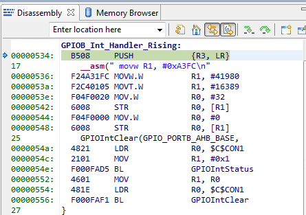
I'm using EK-TM4C1294XL evaluation kit to measure delay between rising edge on PB3 pin and interrupt response. Here's the code:

#include <stdint.h>
#include <stdbool.h>
#include "inc/hw_memmap.h"
#include "inc/hw_types.h"
#include "inc/hw_ints.h"
#include "inc/hw_nvic.h"
#include "inc/hw_gpio.h"
#include "driverlib/interrupt.h"
#include "driverlib/debug.h"
#include "driverlib/fpu.h"
#include "driverlib/gpio.h"
#include "driverlib/pin_map.h"
#include "driverlib/sysctl.h"

void GPIOB_Int_Handler_Rising(void)
{
	__asm("	movw R1, #0xA3FC\n" /*load lower part of GPIOC port addr to r1*/
		  "	movt R1, #0x4005\n" /*load upper part of GPIOC port addr to r1*/
		  "	mov R0, #0x20\n" /* load "on" pin value to r0 */
		  " str R0, [R1]\n"  /* write value of r0 to GPIOC port */
		  "	mov R0, #0x0\n" /* load "off" pin value to r0 */
		  "	str R0, [R1]\n"  /* write value of r1 to GPIOC port */
		  );

	GPIOIntClear(GPIO_PORTB_AHB_BASE,
			GPIOIntStatus(GPIO_PORTB_AHB_BASE, true));
}

void main(void)
{
    uint32_t sys_clk = SysCtlClockFreqSet((SYSCTL_XTAL_25MHZ |
                                             SYSCTL_OSC_MAIN |
                                             SYSCTL_USE_PLL |
                                             SYSCTL_CFG_VCO_480), 120000000);

	SysCtlPeripheralEnable(SYSCTL_PERIPH_GPIOB);
	while(!(SysCtlPeripheralReady(SYSCTL_PERIPH_GPIOB)));

	SysCtlPeripheralEnable(SYSCTL_PERIPH_GPIOC);
	while(!(SysCtlPeripheralReady(SYSCTL_PERIPH_GPIOC)));
	FPUStackingDisable();

	GPIOPinTypeGPIOOutput(GPIO_PORTC_AHB_BASE, GPIO_PIN_5);
	GPIOPadConfigSet(GPIO_PORTC_AHB_BASE, GPIO_PIN_5, GPIO_STRENGTH_8MA_SC,
			GPIO_PIN_TYPE_STD_WPD);

	GPIOIntRegister(GPIO_PORTB_AHB_BASE, GPIOB_Int_Handler_Rising);
	GPIOIntTypeSet(GPIO_PORTB_AHB_BASE, GPIO_PIN_3, GPIO_RISING_EDGE);
	GPIODMATriggerEnable(GPIO_PORTB_AHB_BASE, GPIO_PIN_3);
	GPIOIntEnable(GPIO_PORTB_AHB_BASE, GPIO_INT_PIN_3);
	IntEnable(INT_GPIOB);
	
	while(1);
}

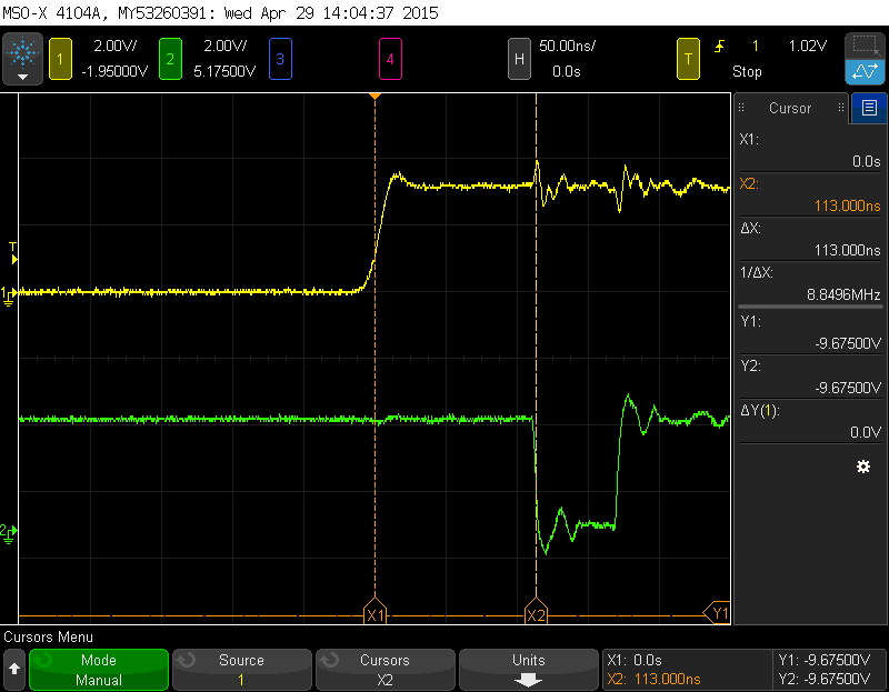
This is what I see on oscilloscope:

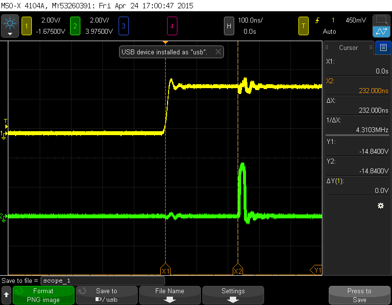
As far as I'm aware, it takes twelve clock cycles to launch interrupt service routine, my assembler code takes another five clock cycles (four to execute and one cycle for gpio pin rise delay) to execute. Together we have seventeen to eighteen(if rising edge on PB3 arrives when system clock is high) clock cycles. System clock runs at 120 MHz frequency, so its period is 8,333 ns. This gives 18 * 8,333 = 150ns of the delay. But on the scope I see about 230 ns of the delay, so where's missing 80 ns?

  • Hi BT,

    I wonder if what you are trying to achieve would not be better executed if using the DMA.

    Either way did you check in the disassembly how may cycles your interrupt takes until the GPIO state is set?
    Do you have FPU enabled?
  • I thought about DMA too, but at first I wanted to try with interrupts. I did check the disassembly, and it looks like this:

    I believe the PUSH instruction cycles belongs to twelve cycle delay to launch interrupt routine, but I'm not sure. Either way, next five cycles is the delay to set the pin to high state.

    FPU is disabled.

  • Thanks for the screenshot BT,

    Do you consider the delay time of a read? The GPIO needs to read and acknowledge the rising edge and call the interrupt. You are working with very small time intervals, consider that the GPIO could consider the rising edge after 2-3 cycles with the input being HIGH.

    You could try to set the optimizer options to higher code speed.
  • Like your general logic & execution - but for your choice - & use - of JTAG "burdened" Port C.  

    Now you/I are aware that you're "banging" PC_5 (outside of JTAG's lower residence w/in Port C) yet still - that port's construction and/or implementation may not (truly) prove "standard!"    Would It not prove "safer - and at least more normal/customary" to run that test upon another port?

    May also prove of use/instructive to "unregister" Port B interrupt - and repeat your test.

  • I've checked delays using pins PE5 and PA7. Results are identical. What do you mean by "unregistering" interrupt?

  • (Take this answer with a grain of salt, it's stuff I've read about and though I've understood, but never tried myself - no need has arisen yet to do that.)

    Did you account for the flash delays? For fast CPU frequencies the flash can only accommodate reads at half the CPU speed. Executing from RAM might save you some clock ticks.
    Also, are all interrupt handlers registered with *IntRegister or "allocated statically" in the startup file? The static method is quicker because the CPU can then read the ISR address in parallel to pushing the CPU registers to the stack as they are in different memory "devices". Having just one *IntRegister call would move the vector table to RAM and the parallel access advantage would be lost.
  • _BT_ said:
    What do you mean by "unregistering" interrupt?

    Allocating that interrupt "statically" (via placement w/in startup file) - nicely detailed (above) by Veikko - usually improves such code execution.

  • Well, I've just tried that, and in fact it even increased the delay by about 10ns. How do I configure CCS project to load code entirely into RAM so I can avoid flash delays?
  • Our firm works w/many ARM MCUs (hard to believe that "single source" is (always) best) and as such avoids the (additionally limited) CCS in favor of more established - multi-vendor accepting IDEs - such as IAR & Keil.

    You can gain real detail by studying this vendor's various "bootloaders" (which cause code to execute from w/in RAM) and also via Joseph Yiu's definitive text on the ARM M3. (substantial carry-over)

  • Well, I think I just take the DMA approach, which gives me little bit less than 100 ns of the delay between interrupt trigger and response which is better than I need.

  • Cool, so you could say that the DMA takes about 12 cycles from when it receives the trigger, to actually finishing the transfer (maybe 11 since the GPIO takes 1 cycle to update the output?)
  • Not exactly, DMA transfer triggers much faster, but transfer is, for some unknown for me reason, slower.

    In above example my transfer is two bytes length, first 0x0, then 0xF. As you can see it takes about 60 ns to switch from low to high state. It's not a problem for me, since I need low latency, speed is not so much important.

  • _BT_ said:
    takes about 60 ns to switch from low to high state.

    Scope trace is so powerful - crystal clear - yet would not that ~60nS have been better illustrated if "X1" replaced "X2" (that's the fall of Ch 2) and "X2" moved to (the rise of Ch 2)?    (thus enabling the "auto-cursor based" time measure)

  • Well, maybe, but when I took this picture I was measuring the delay. Anyway, there is a grid, and time base can be seen, so no problem for me.

  • Indeed that's a nice scope - the automation features both speed & insure correct measurment - (often) preventing (visual) miscues.