This thread has been locked.

If you have a related question, please click the "Ask a related question" button in the top right corner. The newly created question will be automatically linked to this question.

Tiva C flashing with development Kit.

Other Parts Discussed in Thread: TM4C123GH6PGE

Hi,

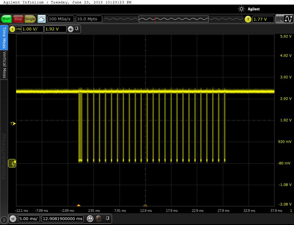
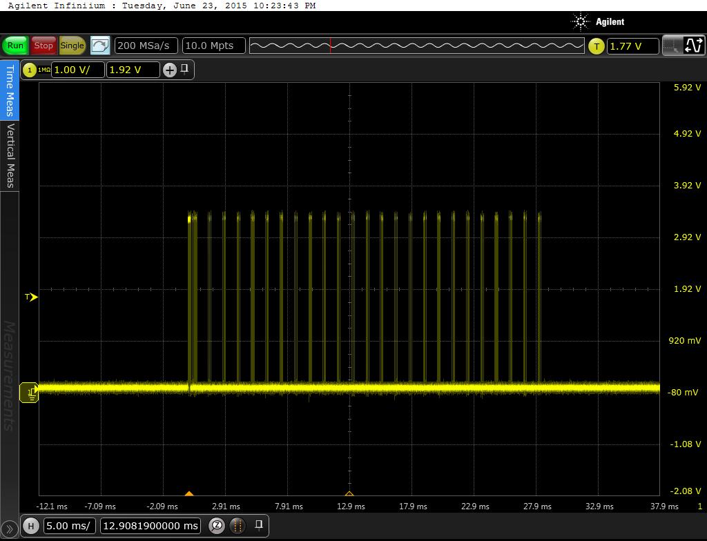
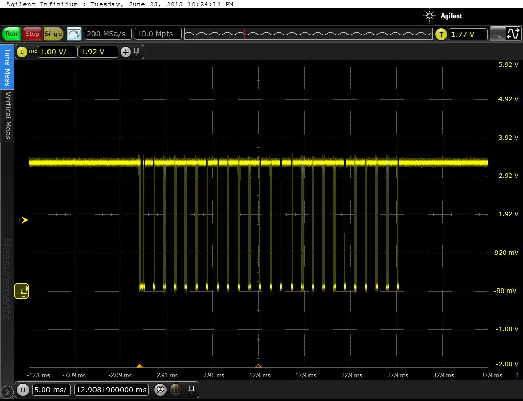
I am using the tm4c123gh6pge MCU, I am trying to flash it with the Tiva C development. When I connect the kit to the board, the JTAG pins TWS, TDI and TDO voltage drop to 2.5 V. However is the PINS aren't connected to the dev kit, the voltage are correct at 3.3 V because of the pull-up

  • Hello Mathieu,

    1. Make sure that the GND is common between the two boards
    2. There must exists a path for the current from the pins to the VCC of the custom board (via resistors or forwardd iode) causing a parasitic current drain and voltage to drop on the IOs.
    3. Make sure that the second board is powered from an independent power supply with sufficient current capacity.

    Regards
    Amit
  • Hi,
    I resolve the issue of not entering debug mode. I checked very carefully with our microscope and I find a little tin passage between TDI and TMS on old tracks I don't use anymore
  • Hi,

    right now I go into FaultISR because I think i didn't set the clock well, if I just want to use the internal clock, is this appropriate:
    SysCtlClockSet(SYSCTL_USE_OSC | SYSCTL_OSC_MAIN);

    [EDIT]

    I use the debug and go trhought line by line and the following line:

    GPIOPinTypeGPIOOutput(GPIO_PORTK_BASE, GPIO_PIN_0|GPIO_PIN_1);

    cause the MCU to go into FaultISR

  • Hello Mathieu,

    Have you enabled the Clock to GPIO Port K. Also please use the full definition of crystal and divider in the SysCtlClockSet function

    Regards
    Amit
  • Hello Amit,

    the problem restart to occur. I am starting that I could have damage the Chip when I tried to programm it with blackhawk debug probe. Is there a way to test the chip and make sure everything is allright? All my power supply VDD and VDDC have correct value but still it is
  • Hello Mathieu,

    You can use a Boundary Scan to check if all IO;s are OK and not shorted. There are different vendors for BSDL debugger and software and the bsdl file are available at www.ti.com for the different TM4C devices. I have used XJTAG (though note that these tools may be expensive).

    The other option is to toggle IO's and check if they swing 3.3V to 0V w/o affecting adjacent IO's (very tedious and painful process if not careful). This method will however not cover the JTAG IOs.

    Regards
    Amit
  • Hello, thanks for the reply, I will look into that. Also do you have a pdf that show step by step how to programm with a development kit?
  • Hello Mathieu,

    Unfortunately no. I do not have a step by step programming of a TM4C device with any of the kits. Normally, I just have the images for connection with instructions that I post on the forum

    Regards
    Amit
  • Hi,

    I understand that. On my custom PCB some VDD Cap are pretty far from their VDD pins. What are the possible errors that it could cause?
  • Hello Mathieu,

    There are 2 sets of caps. A smaller cap for decoupling transients and a larger bulk cap for rapid current increase which an LDO may not respond to. Which one of the two are farther away. On the VDD I would not be much concerned as the supplies usually are good. If this is the case on VDDC then I would be very very concerned. I guess you should have gone through the System Design Guidelines for placement of the caps.

    Regards
    Amit
  • Hi,
    My big cap of VDDC is near the pin 126 (3.3 uF), but my cap on VDD are pretty far from the pin.
  • Hello Mathieu,

    Ouch. Did you check the System Design Guidelines Application Note?

    Regards
    Amit
  • Hi,

    in the datasheet p.1430, the note A recommend that it should be connected near pin 126. It is the same written in the guideline that refer to datasheet p.21
  • Hello Mathieu,

    Note that it is not just one capacitor. It is a set of caps.

    Regards
    Amit
  • Hi,

    so if I only put 1 cap of 3.3 uF, the MCU will most likely bug and not work?
  • I put some small 0.1 uF near the orther VDDC pin too.
  • Hello Mathieu

    Based on the issues so far, I would suggest a clean up of the schematics and layout as per the guidelines.

    Secondly on the non working board, check the tracks for any further shorts.

    Regards
    Amit
  • Hello,

    for the second iteration indeed I will follow more closely the PCB guidance line. I am probing my TCK/TMS/TDO/TDI. I got clear 1 and 0 exchanging between the device and my PC, but there isn't any exchange on TX/RX
  • Hi,

    I got the binary exchnage during the programming:

    TCK

    TMS

    TDO

    TDI

  • Hello Mathieu

    At such resolution is almost impossible to notice anything. You would need to check the first capture of the 4 JTAG lines in higher resolution to see if they match up or not (if there is a short)

    Regards
    Amit
  • Hi,

    so I need to check if the first pulse match for evey signal?
  • Hello Mathieu

    Look for the first 40 bits w.r.t TCK. The signature should be unqiue.

    Regards
    Amit
  • Should not this be handled by one more experienced at, "Université Laval?"

    Really - the design of a pcb - nearing 30 "back-forth" posts - will this ever end!     Should not the school show (some) interest?

    Forum so needs a, "Slaughter Rule!"   (after 20 non effective posts - DONE!)     Get the school involved!!!

    Before hating this reporter - does the, "lack of any progress" - reflect w/great favor upon this school?    Can this be good?    Surely one (school person) more skilled & experienced - can at minimum - "SHARE" this burden w/Amit!  

    Note that by "accepting" such, "endless - progress-lite posts" are not yet more (strongly) encouraged?    What then?    (is it not fair - even proper/responsible - to ask?)

  • Hi,

    yeah It is getting pretty ridiculous for the post lenght. I agree with you CB1. I will try to find resources in my direct environnement.
  • Mathieu - may I applaud your attitude?    Reveals a maturity - and that you are now willing to accept, "reality." 

    My writing was not, "being mean" - but to petition for a more "in depth & experienced review of your board" - most likely from an instructor or similar.

    My small tech firm encounters situations such as yours far too often - so much that I've coined the term, "Maximum Randomness" (to describe).

    Any and Everything is suspect!   Bringing up a new pcb - most always, "Proves an adventure."   It's unlikely that you've designed & implemented "many" in the past - and we note that you discovered the "board design guide" only (after) building your board.

    I'd look now at your justification for a completely, new board - especially one bearing a fine pitch MCU.   Would it not prove simpler & faster to use the LPad with a far simpler, smaller board of your design?   In that manner most of the critical, "Heavy Lifting" has been done for you - you only add the additional capabilities and/or signal routings which you (uniquely) require.

    As a counter to, "Maximum Randomness" our firm always strives to, "Reuse past/proven pcb segments & groupings, always check & double check for vendor "design guides", and give great & careful attention to board, "Test & Troubleshooting" UP FRONT!   (not - as we see far too often - as a way belated, "after-thought!")

    New software, a brand new pcb, first use of components (some exotic) too often results in, "Houston - we've got a problem!"

  • Hi,

    I got into this position because of a faulty design caused by a lack guidance into the fabrication(I didn't know about the PCB guidance when making the PCB) of the PCB resulting a "blindshoot" that fail 99% of the time. MCU's PCB aren't a trivial thing to accomplish. I made PCB in the past but the applications didn't require such precision and knownledge as a MCU does.

    What is the Lpad you are refering too? You mean a smaller MCU from the Tiva C family?

  • By LPad I mean "Launch Pad" - this vendor's small, low cost, Evaluation board.   

    It does the "heavy lifting" of MCU placement, reflow - which frees you to focus upon anything else you wish to add to its features or connectivity.

    In this manner you "escape" the difficult - and may far better concentrate upon adding capability or organizing connectivity - or increasing power handling etc.