This thread has been locked.

If you have a related question, please click the "Ask a related question" button in the top right corner. The newly created question will be automatically linked to this question.

TM4C1294 blocking access to EEPROM (idle mode) auto increments EEOFFSET ring cyclic even if not accessing EERDWRINC.

Guru 55913 points

First like to point out a similar issue was previously posted in this link.

https://e2e.ti.com/support/microcontrollers/tiva_arm/f/908/t/359429

 Datasheet: 8.2.4.1 BLOCKS

The current block is selected by the EEPROM Current Block (EEBLOCK) register. The current offset is selected and checked for validity by the EEPROM Current Offset (EEOFFSET) register. The application may write the EEOFFSET register any time, and it is also automatically incremented when the EEPROM Read-Write with Increment (EERDWRINC) register is accessed. However the EERDWRINC register does not increment the block number, but instead wraps within the block.

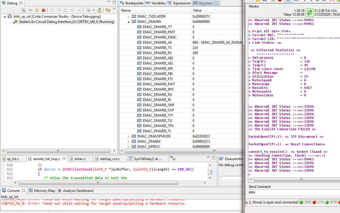
Is it plausible the local bus is accessing the EERDWRINC register when the EEPROM is idle or some kind of refresh is occuring?

We have a Boolean switch block any EEPROM reads after an SRAM array has been filled with data as to block future reads from EEPROM. CCS debug when EEPROM is actually being read EEOFFSET register has random addressing values and not  in a cyclic ring form (-->0,2,4,6,8,A,C,E-->). That same cyclic EEOFFSET ring occurs when ever the application is Paused or during an MPU fault condition. The EERDWR appears in a constant refresh cycling mode following EEOFFSET.


  • Hello BP101,

    Are the EEPROM Registers open in the memory or register window?

    Regards
    Amit
  • Registers window and the offset address cycling is all in block 0.
  • We suspect that Amit's "fearful" that if your EEPROM Registers are "open" w/in your IDE - that may be the cause of your observation.
    It's unclear if you've answered his question...
  • The registers are open in debug while the application is running and in register refresh order we can reveal what and why. This appears to be undocumented EEPROM idle behavior in block 0. The question is how to make it stop cycling addresses without disabling the peripheral.
  • Hello BP101,

    Ensure that EERDWR and EERDWRINC are not in the IDE register window.

    Regards
    Amit
  • Hi Amit,

    Disabling those two registers stops the offset addressing but to what point. We need to know is SW is actually reading the EEROM after blocking SW from repeatedly reading EEPROM. The only noticeable difference is the EEOFSET addresses appear more random without SW blocking.

    So you are implying the simulator is spoofing the registers causing the EEROM to increment the offset address?


  • BP101 said:
    So you are implying the simulator is spoofing the registers 

    Perhaps you intended, "IDE" rather than simulator?

    I believe that Amit is, "sounding the alert" that certain MCU registers must not be allowed to appear w/in key IDE windows as the IDE's "access" of those (relatively few) critical registers may prove disruptive and/or not provide valid data.

    Even "pro IDEs" (such as Keil, IAR) suffer under this limitation - you might do well to consult w/your IDE vendor to see if any workaround is available...

  • Hello BP101,

    I believe so. Look at this way: there are peripheral Data Register which are RO, e.g. UARTDR. When using a FIFO in UART reading the UARTDR pulls one data element from the FIFO, If both the debugger and the CPU are reading the register then one read from the debugger would mean that the CPU will get one less data.

    Regards
    Amit
  • Hi Amit,

    While your answer is clear & consistent - what can this poster - and others - do when confronted with, "Need to Know?"

    Poster Brett here believes he (really) needs that data - yet the IDE "spoils" as you mention - and would not his adding program code to regularly "read" invalidate that key/critical data - as well?

    Suspect that's the (real) issue - and I'm equally - w/out a work-around...

  • Hello cb1,

    There is no WA as the controlled read of the CPU program and the IDE has no means of syncing or blocking each other.

    Regards
    Amit
  • Perhaps you intended, "IDE" rather than simulator?

    My understanding is debug is a remote simulator built into IDE and connects to the ARM cortex simulator, a mirror of the actual registers delivered to debug GUI simulated registers by debug refresh cycles reading the DAP.

    Below Amit seems to believe the debug simulator may some how be triggering EERDWRINC just by reading the cores mirror bits. As you pointed out that is counter productive and also spoofs the user to many head scratching intervals. I don't believe the MPU would ever get one less data rather the ARM simulator submits to the higher priority. That case the debugger gets no read status mirror of the register bits in those higher priority cycles.
  • Hi Amit,

    I don't believe poster's use of "simulator" to be correct/proper here.

    While the IDE - under some circumstances - may be ordered into a "simulator mode" (i.e. primarily when no HW is available) that is NOT the case when the IDE is attached to a real MCU - and the program is up/running!

    And - why would one "want" to simulate - with the delays & uncertainties that introduces - when the REAL hardware is, Right There?   In my firm's experience - simulators most always prove "second" to real HW!

    Further - if the MCU was being "simulated" - would not it then "escape" the (apparent) issue you've noted?  (as the register access is only being, "faked!")
     
    Might you be so good as to comment, Amit?    Merci.

  • Hello BP101,

    I will list my points 1-by-1 and you can correct me when I go divergent.

    1. You are running an application on TM4C1294 which is an actual physical HW device on the other side of a USB cable.
    2. The IDE is connected to the Cortex M4 via the DAP.
    3. You have opened a Register/Memory window which maps into EEPROM Space with Auto Refresh Set.
    4. The EEPROM read is inconsistent when the Reg/Mem Window is open
    5. The EEPROM read is inconsistent when the Reg/Mem Window is closed.

    Regards
    Amit
  • Hi Amit,

    Correct is 4 Open and the two registers you mention to disable are default as enabled.

    @CB1

    Perhaps should say trace buffer but have read WIKI that CCS debug module is a simulator. Retrospect the words (memory mapped trace buffer simulator) seem fitting, yet a mouth full.  Since the trace data are not actually real time events being refreshed in the debug register view pain it seems more fitting to simply say simulator. Think word emulator would infer more of a hardware replacement or emulation. schema. The HW Trace Analyzer can be invoked in debug yet below the JTAG debug register view is not fully explained in that it appears to be using the trace SWO ported data.

    Integrated Configurable Debug:
    The Cortex-M4F processor implements a complete hardware debug solution, providing high system visibility of the processor and memory through either a traditional JTAG port or a 2-pin Serial Wire Debug (SWD) port that is ideal for microcontrollers and other small package devices. The Tiva™ C Series implementation replaces the ARM SW-DP and JTAG-DP with the ARM CoreSight™-compliant Serial Wire JTAG Debug Port (SWJ-DP) interface. The SWJ-DP interface combines the SWD and JTAG debug ports into one module. See the ARM® Debug Interface V5 Architecture Specification for details on SWJ-DP. For system trace, the processor integrates an Instrumentation Trace Macrocell (ITM) alongside data watchpoints and a profiling unit. To enable simple and cost-effective profiling of the system trace events, a Serial Wire Viewer (SWV) can export a stream of software-generated messages, data trace, and profiling information through a single pin.

    Macrocell is Mirror imaging?

  • BP101 said:
    have read WIKI that CCS debug module is a simulator

    I do not find such claim appearing w/in the literature of "Pro/Real" IDEs such as Keil and IAR.   Might you link to that Wiki?

    Again - we were long taught to employ "simulator" only when HW was unavailable - there are (most always) weaknesses & compromises which result when, "simulating."

    I've asked Amit to enrich us w/his comment - my firm's findings cannot support your use of "simulator" w/in your past posting.  

    To highlight the (obvious) limitations of "simulation" - how do you propose one simulate the DAC output (present upon many such M4 MCUs), or the PWM Generator's output, or an ADC's response to a signal input?   (to list - quickly - just a few...)

  • Hello BP101,

    Device simulator as cb1 stated is when the HW is not available. If you have a end board to debug the simulator mode is not what an IDE does. It actually goes for the interaction with the end CPU and the system peripheral.

    Regards
    Amit
  • BP101 said:
    Perhaps should say trace buffer but have read WIKI that CCS debug module is a simulator.

    I would be surprised, nay shocked, if that were the case.

    You can (sometimes) get that kind of behaviour in a bound-out ICE but I've never seen a JTAG setup on a micro with that kind of access to the peripheral internals. It's one of the weaknesses of a JTAG compared to a 'real ICE'. The trade-off of a much cheaper more general purpose debug instrument is probably worth it.

    Even a bound-out ICE would not provide you with 'simulated' results.  The whole strength/purpose for being is to provide real values. A bound out ICE works by providing a replacement core with more debug hooks brought out to the simulator, disabling the core present on the board.

    If you read any register in both your debugger display and program expect any side effects that occur from reading to happen regardless of whether the read happens from the debugger or the program.

    Robert

  • May this reporter offer thanks to both Amit and to Robert.

    While denying "Lone Ranger" status - some here express viewpoints (perhaps unlikely) found w/in multi-person, experienced groups... (sometimes such is described as a, "reach!")
  • Hi Robert,

    Not sure what ICE is exactly. The data in the CCS debug register view in continuous refresh mode is not providing us with real time peripheral register events. Therefore events become buffered and replayed or more simply simulated events that occurred sometime in the past 100 or so milliseconds or even long as few seconds in the past.

    Don't even believe that JTAG has direct access to any peripheral registers other than Flash memory. JTAG uses GPIOC port pins but that only gets us into TRONS universe. The Trace Macrocell more fittingly delivers the registers results to the JTAG port pins. Seems figure 2.1 left out the SWO serial trace data leading back to JTAG and we have to guess this part.
  • Hello BP101

    JTAG has access to the peripheral register via the DAP. If not then how can one set a GPIO Data Register and expect the pin corresponding to it to become high.

    Remeber that the CPU bus is 32 bit @ System Clock but JTAG is a serial Stream @ TCK (with overhead of IR and DR), which would make it way slower and refreshes not that fast.

    Regards
    Amit
  • BP101 said:
    Not sure what ICE is exactly.

    In Circuit Emulator. Still used on micros w/o JTAG but has generally been replaced with JTAG emulation of ICE on micros with JTAG support. A little more powerful, a lot more expensive. 

    BP101 said:
    Don't even believe that JTAG has direct access to any peripheral registers other than Flash memory.

    Au contraire, that's French for on the contrary.1

    You have a broken mental model of how JTAG works, even on chips like FPGAs it accesses the internal registers, that is the magic that makes it work.

    Robert

    1 - Forgive the Dead Dog Café reference

  • "JTAG has access to the peripheral register via the DAP. If not then how can one set a GPIO Data Register and expect the pin corresponding to it to become high."

    Not sure how that can be possible since all that ICDI can do in CCS debug is read the DAP for slower than ever register event updates and write flash memory addressed data with the application object. The MPU executes the application object which eventually asserts the GPIO port pin High not directly via the JTAG port.

    The diagram posted above shows the JTAG pins have access to the DAP which arbitrates data flow onto the local bus in order the flash memory can be written with the object code. If there is some utility that allows JTAG or ICDI to have direct access to registers then we should be receiving near real time updates in the CCS debug registers window. My Intel quad core 2.8GHz processor is pushing the USB data from the ICDI into the CCS debug at break neck serial speed 250KBPS. Have heard other over clockers state they double that USB v.2 speed. 

    "Remember that the CPU bus is 32 bit @ System Clock but JTAG is a serial Stream @ TCK (with overhead of IR and DR), which would make it way slower and refreshes not that fast."

    The trace macro cell is also slow to retrieve every event change in all the peripheral registers and mirror all that data up the DAP. Seems if the debug had direct access to register the EEPROM should not be incrementing the EERDWRINC just by reading the idle register. BTW the USB 0-7 FIFO's are doing the same thing and no serial data is entering or leaving the OTG port.

  • Hello BP101

    BP101 said:
    Not sure how that can be possible since all that ICDI can do in CCS debug is read the DAP for slower than ever register event updates and write flash memory addressed data with the application object.

    That is not true. If the DAP can access flash then so it can access the GPIO registers.

    BP101 said:
    The MPU executes the application object which eventually asserts the GPIO port pin High not directly via the JTAG port.

    If the flash is erased,even then the DAP can be used to access peripheral registers once the clock is enabled by writing to the appropriate SYSCTL.RCGCxxx register.

    If you go through the ARM DAP Debug Architecture specification (requires a lot of patience and time to understand the document) you would realize how debug via an IDE works. It is out of personal experience that I can say that and having created my own debug application.

    Regards

    Amit

  • BP101 said:
    Seems if the debug had direct access to register the EEPROM should not be incrementing the EERDWRINC just by reading the idle register

    You've misunderstood, it doesn't have access to the EEProm (or any other external peripheral) internals. It accesses them through the data bus just as the micro does.  The JTAG is integrated with the micro Core by ARM, the peripheral, including memory, are provided by TI. As such the only internal representations the JTAG/Debug core has access to are the core's and even that generally appears to be limited.

    As far as the peripherals are concerned, the JTAG appears to behave like a microcontroller accessing their exposed registers. And keep in mind that in a number of these registers probably do not keep any sort of internal mirror.  The EE address register is probably one of those.

    Robert

  • Note this explanation is my own mental model. If you really need details (as opposed to just working with a debugger) then you should follow Amit's suggestion and actually read through all the technical implementation details.

    Robert
  • As such the only internal representations the JTAG/Debug core has access to are the core's and even that generally appears to be limited.

    That is exactly my point the ARM trace macro cell is the core trace storage for the vendor provided peripheral interface on the local bus. All vendor related peripheral data is monitored by the trace macro cell and ported up to the DAP. That way any vendor peripheral caused precise bus exception and processing is handled by the MPU core when the trace cell detects error in the vendors data stream. Otherwise the core would crash and the MPU halt anytime the vendors peripherals or ICDI/JTAG debug interject unscrupulous data on the local bus. There are many core register settings one is to have the MPU keep running during an exception event. One such core option allows priority write access to protected vendor registers. NVIC interrupt register for setting SW interrupt triggers. 
     
    Never suggested the ICDI had access directly to the EEPROM peripheral addresses . If JTAG can directly access and set bits in the vendors peripheral registers as Amit suggests then why doe CCS debug have issues to properly follow the registers events. The best explanation is the ICDI register event data is disconnected mirrored history. The entire argument lies on the point the EEPROM is no longer being accessed by the application in so the EERDWRINC should not by design be Self incrementing offset address inside block 0. USB0 is doing the very same thing with FIFO registers 0-7 addresses cycling like mad when no external OTG activity. That behavior also infers the CCS debug and ICDI/JTAG is not directly in contact with the vendor provided peripheral registers.

  • BP101 said:
    If JTAG can directly access and set bits in the vendors peripheral registers as Amit suggests then why doe CCS debug have issues to properly follow the registers events

    Because it is reading a register that auto-increments when it is read.  To keep the data up to date it has to re-read the register. That is a direct consequence of reading the peripherals exposed registers with no access to the internals (although I doubt deeper access would help).

    BP101 said:
    Never suggested the ICDI had assess directly to the EEPROM peripheral addresses

    But it does, that's how it works. It directly accesses the EEProm's registers via the data bus.

    BP101 said:
    USB0 is doing the very same thing with FIFO registers 0-7 addresses cycling like mad when no external OTG activity.

    That's what I would expect

    BP101 said:
    That behavior also infers the CCS debug and ICDI/JTAG is not directly in contact with the vendor provided peripheral registers.

    The other way around

    BP101 said:
    The entire argument lies on the point the EEPROM is no longer being accessed by the application in so the EERDWRINC should not by design be Self incrementing offset address inside block 0.

    The EEProm cannot distinguish between a register read by the application and a register read by the debug core.

    Some bond-out ICEs could make that distinction on peripheral access but I don't think I've ever heard of a JTAG debug core that did.

    Robert

  • Hello Robert,

    I echo-ed the same, as well in my post. Just to add to the content of this thread, there are ways of making the peripheral know whether it is a debug or application access and alter the behavior of the peripheral. But this requires substantial HW logic to be placed and more than that testing to ensure that it does not break an application.

    Regards
    Amit
  • Hi Amit,

    "If the flash is erased, even then the DAP can be used to access peripheral registers once the clock is enabled by writing to the appropriate SYSCTL.RCGCxxx register."

    Agree in part with what your stating but it seems that JTAG /ICDI is not in direct access to or with the vendor provide registers even if the DAP has direct access to the local bus. No ARM diagram or proof of such architecture is provided other than a disconnected SWD SWO, where does SWD SWO end up at? Otherwise keeping on topic the EERDWRINC in perspective should not be causing idle mode address offset incrementing in the EEPROM. Else the silicon has a design flaw (unlikely).

    Perhaps when the application is not accessing the peripheral via the local bus the Core trace macro cell ETM is posting a ghost image of the vendor registers up to the DAP via SWD SWO. Best explanation to account for the USB and EEPOM and other registers that have the very same behavior in CCS debug.

    See edits:

  • Hello BP101

    Knowing the Debug Architecture of Cortex M4F and in specific to TM4C12x devices JTAG/ICDI does have access. The information in the Debug Arch Document I mentioned takes weeks to understand. I recently had a call with a customer trying to do the same and it took me 5 hrs to explain the concept of DAP Debug Arch and they are yet no close to being able to write the flasher tool (something which took me 3 weeks almost 3 years back, but to do now takes 3 minutes 3-3-3).

    I can't add any more context and content to this thread, and definitely not any further than what cb1 and Robert also have mentioned.

    Regards
    Amit
  • Some good explanations given but still not totally agree with logic.
    If all that were true than every (idle) addressable vendor register would increment when ever they are read by CCS debug and that is not the case.

    Might it be the DAP posts the vendors register data via SWO and when there is no vendor register activity on the local bus for an enabled peripheral the trace macro cell posts mirrors to the DAP of the snapshot it took of the vendor registers it last stored?

  • BP101 said:
    Some good explanations given but still not totally agree with logic.
    If all that were true than every (idle) addressable vendor register would increment when ever they are read by CCS debug and that is not the case.

    No, only those that are auto-increment on read.  That's a (very) small subset of the registers.

    Note that some registers auto-clear on read, those will have a similar problem if read by a debugger, the information will disappear before the application can read it if the debugger reads it first.

    Robert

  • Ok but the ICDI should not be reading or polling any vendor registers. In retrospect the ICDI should only be receiving updates from SWO when a register changes not the other way around. Definitely do not trust ICDI polling vendor registers directly as that can take clock cycles away from the application or even cause it and debug to hang if the timing is iffy. Have had that occur several times in last few month of tracing reoccurring random exception 11 event, left only wondering what and why. If ICDI is polling that explains much of the quirky debug behavior.

    Read article on ARM web site years ago and got the impression the ARM trace macro cell was ICE for the SWD interface. Have to go back and reread that piece again.

  • BP101 said:
    Ok but the ICDI should not be reading or polling any vendor registers.

    It will if it needs to refresh the display of those registers.  Debuggers can take two approaches, refresh on demand or refresh automatically.  The former usually picked to improve single step performance, the latter removes the need to continually press update.  In either case putting registers that will modify on read in a view window is a bad idea, you either end up looking at stale data or you destroy what you are attempting to view.

    BP101 said:
    In retrospect the ICDI should only be receiving updates from SWD when a register changes not the other way around

    SWD doesn't know when peripheral registers change.  I don't think the built-in trace extends that far.  It 'just' records bus changes.

    BP101 said:
    Read article on ARM web site years ago and got the impression the ARM trace macro cell was ICE for the SWD interface.

    That's the impression they like to leave.  And it does do most of what a full fledged ICE trace does.  I'm not convinced the debug core and the trace core do all that a full ICE does but you are probably never going to see a bond out version of an arm core based cortex, it would be too expensive for the gain in power, even more so since so few would want it.

    Even bond out ICEs generally had the same issue with peripheral registers though, with a few exceptions.

    Robert

    Robert

  • Meant to type SWO not SWD last few posts (back edit). The advance peripheral bus yellow box is the vendor bus in my mind and see how the trace macro cell connects to it, then SWO exits in my mind out to the SWD/ICDI AKA JTAG. 


  • Which does not contradict anything I've said. If you display a register the debug has to read it (trace doesn't enter the picture). SWO is simply the communication mechanism for the results of the debug read.

    Robert
  • The former usually picked to improve single step performance,

    Seem to recall reading application single stepping occurs in the ETM and exits SWO out to SWD/ICDI. We don't actually execute the object from SRAM when stepping into the embedded simulation. Good explanation of why the disassembler view has addresses that differ from the SRAM address range.

    Given that data passes out the TPU it would seem plausible the debug registers view could also be receiving update data from the TPU.
  • BP101 said:
    Seem to recall reading application single stepping occurs in the ETM and exits SWO out to SWD/ICDI.

    That sounds like a reasonable place to control single stepping. Although exits SWO doesn't parse for me.

    BP101 said:
    We don't actually execute the object from SRAM when stepping into the embedded simulation.

    Well I would expect normally you would execute from flash.  Single step can be executed via breakpoints but I understand that this core has support to set the processor to single step mode and have it halt after each instruction so you can single step flash (or ROM) without needing a RAM copy.

    BP101 said:
    Good explanation of why the disassembler view has addresses that differ from the SRAM address range.

    If your application is actually in SRAM you should see SRAM addresses in single step.

    BP101 said:
    Given that data passes out the TPU it would seem plausible the debug registers view could also be receiving update data from the TPU.

    The TPIU is just a data port, not much intelligence. Any register you see must be read via an explicit read.

    Note that the ITM and ETM only have connections to the core so they cannot even 'see' peripheral registers.  You might not need to go through the bus to access the CPU registers. The TPIU has connections to the bus it can be used as a communications port for the DAP and application.

    Robert

  • >>Well I would expect normally you would execute from flash.

    Never have seen 0x2xxx.xxx even with the boot loader installed which copies the flash application object into SRAM and executes the code from SRAM. We have to use the memory viewer in CCS debug order to see a valid memory map.

    >>Single step can be executed via breakpoints but I understand that this core has support to set the processor to single step mode and have it halt after each instruction so you can single step flash (or ROM) without needing a RAM copy.

    The point being made was the application object is being single stepped in the ITM/ETM at the instruction decoder level after each instruction prefetch cycle. That classifies it more like an ICE. Some of us back in the day had CPM machines with wire harness hot to CPU socket of the target achieving similar stepping results and peripheral register control to boot.

    >>The TPIU is just a data port, not much intelligence.

    The arrows of bus data flow point from the APB (vendor peripherals) up to the TPIU out via SWO and not from the APB out to the SWD. Think more is going on here with the reading of vendor registers than some are believing possible.
  • BP101 said:
    >>Well I would expect normally you would execute from flash.

    Never have seen 0x2xxx.xxx even with the boot loader installed which copies the flash application object into SRAM and executes the code from SRAM. We have to use the memory viewer in CCS debug order to see a valid memory map.

    That sounds like a bigger problem.

    Mind you if you are using the ROM based bootloader I don't think there is any necessity to copy it to RAM.

    BP101 said:
    >>Single step can be executed via breakpoints but I understand that this core has support to set the processor to single step mode and have it halt after each instruction so you can single step flash (or ROM) without needing a RAM copy.

    The point being made was the application object is being single stepped in the ITM/ETM at the instruction decoder level after each instruction prefetch cycle. That classifies it more like an ICE. Some of us back in the day had CPM machines with wire harness hot to CPU socket of the target achieving similar stepping results and peripheral register control to boot.

    So? That doesn't invalidate or change any of the previous comments I made. If anything it emphasizes them.

    BP101 said:
    >>The TPIU is just a data port, not much intelligence.

    The arrows of bus data flow point from the APB (vendor peripherals) up to the TPIU out via SWO and not from the APB out to the SWD. Think more is going on here with the reading of vendor registers than some are believing possible.

    You are violating the principle of parsimony1.

    There are two things to keep in mind when reading a manual (particularly a manual for a microcontroller)

    1. If a secondary behaviour is not needed to meet the requirements of another described behaviour you must not expect that secondary behaviour to exist. None of the behaviour you are describing is needed to provide the interface described.  You cannot assume it will be there and experience shows that it is not.
    2. Just because you would have implemented something in a particular fashion does not mean the designers of the core did. And they likely have perfectly valid reasons for designing the way they did.

    Note: that number 1 is a good position both from an abstract point of view from managing expectations and from the view that generally implementation will be as simple as the designer can make them in order to contain costs and produce a testable, proven to work product.

    In summary, according to the documentation (and behaviour)

    • the TPIU acts as a simple interface to the ITM and ETM. In addition it exposes an interface to the peripheral bus that allows the user to make use of the same interface.
    • The ETM and ITM are embedded into the core which gives them access to the core's pipeline and register set so they avoid the side effects of trying to match data bus activity to activity further up the pipeline. They have no access to the peripherals as a consequence.
    • The DAP works though the data bus, not the core. It has access to the TPIU through the data bus and also to the registers on the peripherals.  Since this access is the same as that of the core any read/write behaviour by the DAP is identical in effect to that of the core.

    Robert

    1 - This principle is known by other names, most famously perhaps as Occam's Razor

  • Loved your "tag" - pity it's not a "long-time" standard. (we await the (incoming) salvo...)
  • >>Mind you if you are using the ROM based bootloader I don't think there is any necessity to copy it to RAM.

    The boot loader model always copies it self and the flash stored application into SRAM where it executes both. That is why the start address of the application always exists above BL on a 16KB boundary.

    >>•The ETM and ITM are embedded into the core which gives them access to the core's pipeline and register set so they avoid the side effects of trying to match data bus activity to activity further up the pipeline. They have no access to the peripherals as a consequence.

    Note worthy is CCS debug register view behaves quite the opposite to how you describe. That evidence points to ETM having bidirectional bus access to the ATB via the BM, porting data via SWO and not via BM porting data into SWD. I have proved this in a forum posting shows the UARTprintf() of an active peripheral RW1C register DMARIS that stopped updating the bits in DEBUG register view as the ETM stopped emulating that specific register during debug refresh. Yet other unaffected registers kept refreshing as if nothing was wrong.

    >>•The DAP works though the data bus, not the core. It has access to the TPIU through the data bus and also to the registers on the peripherals. Since this access is the same as that of the core any read/write behavior by the DAP is identical in effect to that of the core.

    Seems to me the DAP works through the bus matrix (BM) much different than just a octal transparent latch onto a local databus. The BM enters the MPU front side bus (FSB) also a bidirectional pipe and the APB has BiDi access to the BM into the FSB sending the vendors register data for debug emulations via the ETM porting results out the SWO ---- the arrows are misleading. The DAP nor the BM has unrestricted direct access to the APB registers during debug emulations as the embedded microcode arbitrates the core data bus and the BM. Perhaps in a custom utility it may be possible to override the ETM default behavior as Amit pointed out but that is not how CCS debug is working.

    The figure posted above is only a simplified model that attempts to keep public disclosure minimal yet the architecture overview text makes the connections not shown in the figure.

  • Below example terminal emulator (right) reports 99461, 32896 and the debug register view is running yet the DMARIS register bits stopped updating. We use the UARTprintf() via CDM virtual COM port data piped out the ICDI into the terminal emulator polling the very same peripheral register, DMARIS. As you can see the DMARIS register is sill quite busy yet it seems the ETM has stopped receiving APB events via the BM resulting in no ETM data being sent to SWO for the DMARIS register. Clearly much more is going on inside the simulator than figure 2-1 makes clear. The DAP seems disconnected from the APB and or BM.

    The ICDI/SWD is not paused rather is still in RUN mode. The console tab messages are left overs from having an register open prior to entering Run mode.