This thread has been locked.

If you have a related question, please click the "Ask a related question" button in the top right corner. The newly created question will be automatically linked to this question.

Tiva C Launchpad problem with external supply

Other Parts Discussed in Thread: TM4C123GH6PM

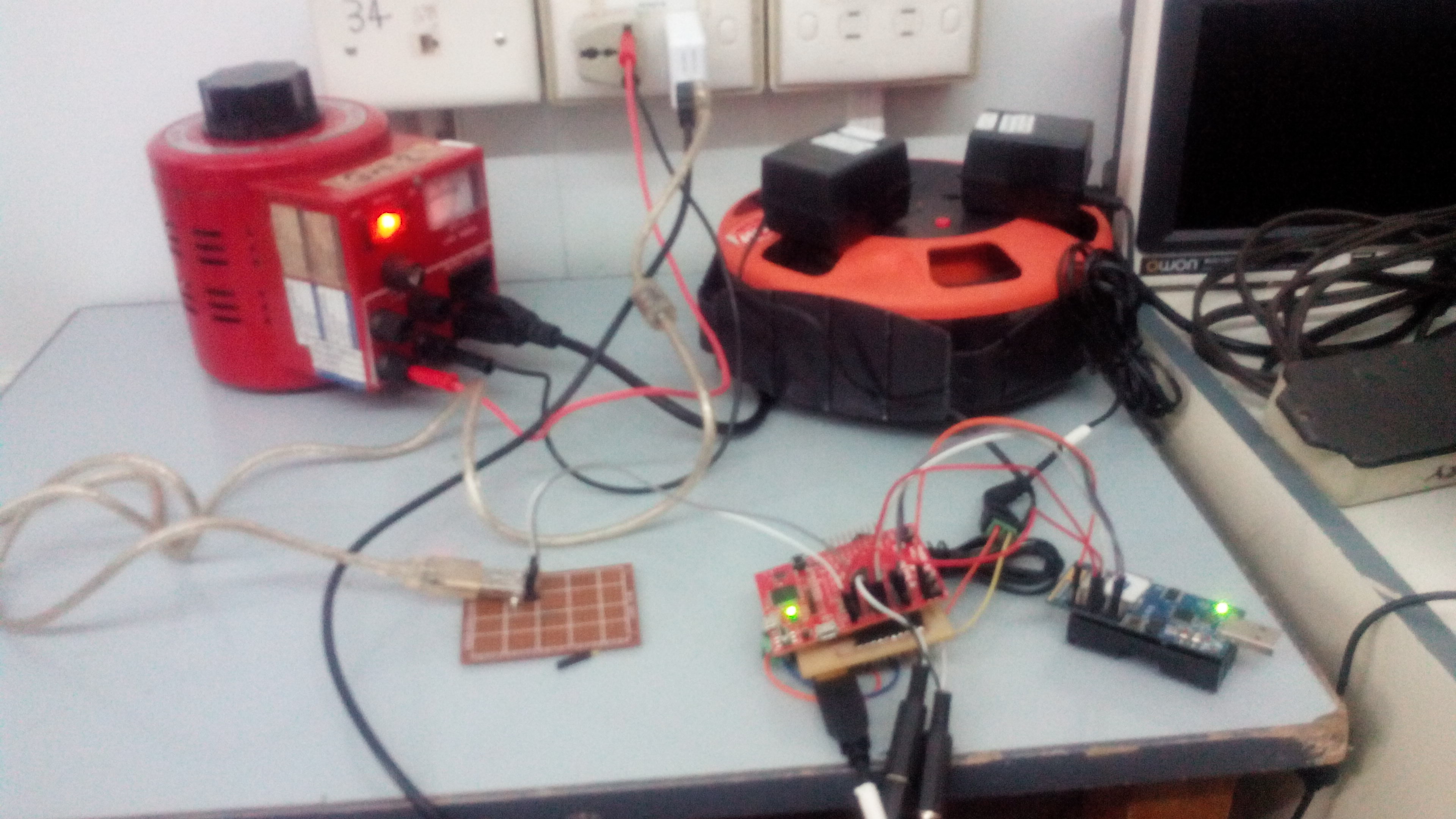
I tried to power my TM4C123GH6PM using a 5V external supply. However, when I do so, the program uploaded to it tends to "misbehave". (The program is simply to collect analog signal and sample it using Tiva ADC - the program is working perfectly during debug mode). Every time I switch back the USB to debug mode, I have to upload the code again in order to correct Tiva's performance.


At the end of the day, it's as if I should stick with using debug mode when deploying my Tiva. Any ideas? (I really need to deploy the Tiva with simply an external 5V supply).


I already consulted the user guide and the datasheet for any reference to device mode or external supply for the Tiva board. So far, I haven't found any good leads yet :)

  • Hello Mark

    How are you providing the 5V to the LaunchPad?

    Regards
    Amit
  • Mark Anthony Cabilo said:
    At the end of the day, it's as if I should stick with using debug mode when deploying my Tiva.

    Perhaps a better "day ending" results w/review of the Eval Board's User Guide.   (strange that)

    Two things are required to meet your goal:

    • Power Switch - top left of your board - in left position.  (Device)
    • 5V (5V0) introduced via J3-1.  (top pin, marked VBus, on your Eval board)

    You (must) supply ground as well - J3-2 (just below the 5V pin) conveniently enables a 2 pin receptacle to provide 5V & Ground...

    Do NOT try to provide 3V3 directly - and insure that the power switch is to the left when powering in this manner.

  • I have a regulated power adaptor (5vdc, 500mA max) typical for USB connection.

  • Hi cb1,

    I already did all that. The eval board's user guide was already consulted. The switch is switched properly. In fact, Tiva is running and the code is executing. The problem is that the expected results from the Tiva changes and becomes erroneous. Only if I switch back to debug and upload the codes again will Tiva perform perfectly well again.

    Just a clarification though.
    My Vbus (J3-1) and GND (J3-2) are used to provide power to another device (TelosB mote). So the supply for Tiva was connected using the "Device" USB micro port. This is when the Tiva would still run yet "misbehaving". Yet all becomes alright if I just stay with using the Debug USB micro port. :)
  • Hello Mark,

    What is the place on the LaunchPad where you are providing the 5V?

    Regards
    Amit
  • I'm connecting the external 5V supply to the device USB port at the left side of Tiva.
  • Hello Mark,

    And was the R29 resistor populated on your board which connects the +VBUS to the PB1 GPIO of the main MCU?

    Regards
    Amit
  • Hi Amit,

    I believe that the R29 resistor is not populated. Do I have to? What does it mean to connect the Vbus PB1 GPIO? I am not using that pin though.

    Thanks.
  • Hello Mark,

    If it is not populated then the suspected issue of damage to PB1 pin due to latch up is not the cause. I will have to try to power my LaunchPad tomorrow in the same manner as yours to see if I can replicate the issue.

    Regards
    Amit
  • Hi Amit, thanks.

    Let me tell you how I set it up here:
    * I connected a 5Vdc, 500mA max external supply to the "Device" USB port.
    * I used the Vbus and GND pins of the Tiva to supply another device
    * I used Tiva's ADC and try to display the results.
    * The sampled values became smaller than expected. When I reconnect the Tiva in debug mode and upload the code, the values are fine again.


    Best regards,
    Amit
  • Hello Mark,

    And at that time the switch is in Device Mode?

    Regards
    Amit
  • Mark Anthony Cabilo said:
    I tried to power my TM4C123GH6PM using a 5V external supply.

    Above - unedited/direct quote - w/in your opening post - is (far) from the (new) facts you add to the mix.

    Nothing in that post indicated that you had read the User Manual.   The info I supplied was absolutely "spot on."

    Adding new info - after the fact - confounds helpers & wastes time, effort, space...

  • Mark Anthony Cabilo said:
    The sampled values became smaller than expected.

    This is important information.  How much smaller?

    Robert

  • Hi Amit,

    Yes, it was.
  • Hi Robert.

    Yes, you are right. I have observed that the value change has a pattern. I expect the result or reading to be 230V but when in device mode the reading becomes around 31-35V.

    Hope this helps.

    Thanks.
  • Umm, since the A/D does not read in volts that's not particularly informative. Probably not helpful for your troubleshooting either since there is a lot that can go wrong between the A/D conversion and the scaled output. The actual A/D values would likely be more useful to both of us.

    Having said that, also useful would be

    • Measured supply voltages (on both supply voltages to micro)
    • Measured A/D input voltages
    • Measured noise levels both on supplies and inputs

    Robert

  • Hello Mark,

    I connected a 5V (arrow 2) and GND (arrow 1) from a 5V bench supply. The switch (arrow 3) is in device mode. I am able to flash qs_rgb example and get it to work no matter how many times I power it ON-OFF-ON (at least 6 attempts).

    Regards

    Amit

  • Hi Mark !

    I was dealing with the same problem until today. I even cut my USB cable's +5v line to exclude any effect the usb power supply has.
    My launchpad could not even start properly without USB connection. SInce I've cut the +5v line in the cable, I begin to think what is the only difference if I connect the cable. There are two data lines remaining and the GND. I figured the data lines could not affect the launchpad, so the next suspect was the GND. And voila ! I connected J3.2 (GND) and the USB's GND and the launchpad came alive without the USB cable. It seems to me that the debug micro does get some power from the external supply, but doesn't get proper GND from it. So I soldered a wire to the USB port's housing (GND), and connected it to J3.2. It solved my problem.
    My setup is similar like yours.
    1. I am providing +5v to Vbus from external power supply
    2. I have cut the USB cable's +5V line (red wire ), to exclude any possibility of supply problems. This way I am able to debug the board while it is
    connnected to external power
    3. I am using launchpad's +3.3V to power some minimal external electronic.

    Edit : It turned out that it doesn't solved the problem, just temporarly, but I think I found the real issue : The power supply I use to provide +5v , doesn't have a chassis ground pin, though it runs from the 220V outlet (220v/5v switching PSU ).. So I connected the wall outlet ground to the launchpad's GND, and also to my metal box, to have proper ground, everywhere, and now it works OK.


    Hope I helped.

    Regards,
    Attila

  • Hi Robert,

    I would try to do your suggestion. If this is anything valuable, would the ADC perform differently if connected to an external supply? I'm not sure about this. Because when I am in debug mode, the ADC, the input, the result, everything works fine.

    Thanks.
  • Hi Amit,

    I tried your setup today. The Tiva is running just as it did last time but the results are still erroneous. It's just the same error as we have been experiencing for a week now. I have a question about the Tiva ground pins (including those GNDs beside SW1 and SW2, and J3-2): are they all connected? I'm sorry, I'm quite confused with the schematic at the user guide right now.
  • Hi Attila,

    I would try this but just to prevent any reckless mistakes in doing so, could you give me some pictures in how you did it? It would really help a lot.

    Also, you mentioned that you connected the wall outlet ground to the launchpad's ground. I'll just do it if I don't have a chassis ground right?
  • Hello Mark

    Yes, they are the same GND. Is it possible, that somehow the power stage is damaged during some manual re-connect. A new launchpad may answer that.

    Regards
    Amit
  • Thanks Amit.

    I will try.
  • Hi Amit,

    We have tried your setup with another Tiva board. The same wrong results appear. I'm sorry, this is really making me frustrated :(
  • Hello Mark

    And when you connect the debugger and connect to the CPU without loading the code, what does the CPU Registers show the code is stuck in?

    Regards
    Amit
  • Pardon - we don't believe his code gets stuck - poster repeatedly reports (only) vastly lowered ADC values when run "outside" of debug.

    My bet is on poster's failure to introduce his 5V via the two pins I identified - my first posting - this thread.   I repeat here - for those (willing) to comply:

    • Power Switch - top left of your board - in left position.  (Device)
    • 5V (5V0) introduced via J3-1.  (top pin, marked VBus, on your Eval board)

    You (must) supply ground as well - J3-2 (just below the 5V pin) conveniently enables a 2 pin receptacle to provide 5V & Ground...

    Firm/I (just like you, Amit) have test/verified - each/every ADC reading holds extremely close - either with - or WITHOUT debugger (J-Link) attached AND w/external 5V brought in PROPERLY!

    Applying 5V-based power to the LPad via the USB cable (appears) to be the culprit.

  • Hi all,

    We've been trying to solve our problem using everyone's suggestion so far.

    The following is our setup here.

    The small adapter in the outlet converts 220V to 5Vdc. It has two USB ports. Our Tiva has a conditioning circuit that converts the voltage transducers output to a range of 0-3.3V for the ADC. We introduced an offset in that circuit to prevent negative-valued voltages and make the minimum value to approximately 0V. That is the black USB connected to the white adapter providing a 5V source for the conditioning circuit. The whitish USB cable is used for Tiva's supply. The blue device beside Tiva is a wireless sensor mote used for transmitting Tiva results to a computer.

    When we switch to debug mode, everything is working fine. The result displayed in the IAR (the IDE we used, debugger is Stellaris, and the values are in decimal) and the results sent over by the wireless sensor (in hex) are the same. Just look into the the hex value that says "01 then FD", the value is "FD" or 253V.

    Before I came to this forum, the result we've been seeing is that the values displayed is smaller than is expected (based from the raw output of the ADC - we even checked the values before and after ADC gain and offset corrections are performed). The value from the IAR and the wireless sensor is still the same but from values ranging "DE-FD" it became "01 or 02" (previously it was "21 or 23"). We just neglect the rest of the numbers so as to be simple.

    Anyways, setup#1 involved Amit's suggestion that he provided with a picture. The switch is in device mode. The ground pins from the either set of headers in Tiva are connected. The Tiva is running and the code is running; however, the result is still that set of low-valued numbers - nothing changed.

    Setup#2 involved cb1's suggestion of powering the Tiva through the J3-1 pin (Vbus) and the J3-2 pin (GND). The switch is in device mode. The result is still the same.

    Setup#3 involved Atilla's suggestion. This part is kind of blurry because I don't understand the way he wanted to ground the Tiva and the external supply. So we open up the microUSB and shorted to ground the pin (pin4, I think it's the shield pin) beside the ground pin. We didn't use the data lines. The setup is similar to cb1's. The result, however, didn't change.

    All of the suggested setups allow the Tiva to run and the wireless sensor drawing power from Tiva also run properly. However, the results being displayed in both the IAR watch (using Stellaris debugger) and the wireless mote terminal are the consistently equal but not correct.
    ---------------------------------------------

    My thoughts regarding this problem are:

    1. It could not have been the wireless sensor connection. Because whether the result is correct or not, it's data and the data output from the Tiva are the same.

    2. It could not have been the Tiva code. I verified what happens to the data if I comment out certain parts of the code (from ADC corrections to power computations for the output). To summarize, the outputs read are consistent with what was missed out. For as long as the Tiva is debugged, the results are correct.

    3. It might be the ground anywhere in the setup. Earlier I asked about the ground pins of the Tiva board, whether they are all the same (analog, digital, etc). If they are all connected, then connecting J3-2 and J2-1 with a jumper wire is redundant. The adapter's ground might be it. I don't know how to verify. The ground in the conditioning circuit connects to the ground of the Tiva board through the two pins (the conditioning circuit was designed like a Tiva shield).

    I observed Vbus can be a source of power or the pin where the power is supplied in.

    If I remove the wireless sensor, the error still persists once I use the external supply (based on the IAR results).

    ---------------------------------------------


    So the question I asked myself at this point is, "What's the difference between the power drawn from the laptop/PC and the power supplied by the adapter?" I measured the current and voltage values and they are the same (5V, 89mA). At this point, I get more confused.

    I went back to the schematic diagrams and noticed the J9 (device mode USB) 5V pin connects to the PB0 with 0ohm resistor but in J11(debug mode USB), the 5V pin is connected to a 330ohm resistor before reaching PB0. Is there something significant about this difference in resistor value? What is it for?

  • Without loading the code, I noticed that the board worked fine. The results are correct.
  • Hi Mark !

    Sorry, I was away for the weekend. Yes, it is useful if you don't have a chassis GND. I realized that my power supply has only 2 connections for 220v, no ground. My 220v ground was connected to chassis, but wasn't connected to TIVA's GND, so the TIVA's GND was somewhere "floating" regarding to the power inlet and chassis ground.
    When I was running it connected to the PC, the USB connector's GND pin grounded the TIVA properly, because I imagine , inside the PC, the USB GND and other GND's are connected. So this way I unintentionally connected the TIVA to the wall outlet/chassis GND.
    The symptoms I had were :
    - The board won't start
    - If it started it halted the program execution after some time
    - Reading false digital input levels ( noise issues I think)

    Regarding how I solved it > I just soldered a fairly thick cable to the USB connector's housing, and the other and directly to my 220v power inlet's ground pin ( which is also connected to my metal box - chassis ground ).
    I can confirm that after proper grounding all problems went away.
    Do you use a laboratory power supply for providing +5v ? Other , especially switching power supplies can have considerably high ripple voltage which can affect everything - but considering your low power consumption it would not be the case.
    I worked with ADC's on several boards like TIVA, and the main issue was always noise. You should check your incoming signal quality with oscilloscope in both cases, measured as close as possible to the ADC pins.
  • From the datasheet :
    "The TM4C123GH6PM target device is also capable of USB embedded host and on-the-go (OTG)
    functions. OTG functionality can be enabled by populating R25 and R29 with 0-Ω resistors. These
    resistors connect the USB ID and USB VBUS signals to PB0 and PB1. When these resistors are populated,
    PB0 and PB1 must remain in the respective USB pin mode configurations to prevent device damage. PB0
    and PB1 are also present on the J1 BoosterPack header. Therefore, if R25 or R29 are populated, care
    must be taken not to conflict these signals with BoosterPack signals."

    So these resistor are not populated by default.
  • You have yet to perform any measurements (at least as far as I can tell). Really at this point you have no idea what the problem even is.

    Robert
  • May I suggest that you introduce, "Known, stable, and common ground Voltages" (w/in MCU's ADC spec) as my past posting urged. We do that on a regular basis - in fact we have a standard, "Test/Verify pcb" which employs a plug-in socket - which then quickly/easily mates with a (common header) which we always employ on our manufactured pcbs.   This small board is capable of generating up to 12 calibrated, known (and adjustable) voltages - to facilitate ADC testing.

    Upon reading of your plight - we did just that - in accord w/my first post, here. And 8 ADC channels responded w/in 5% of expectations - and remained so - in over 2 hours of testing.   Note - we powered (both) our "ADC Calibration board" and the LPad/Eval board from the same (external) 5V source.   Our ONLY ground connection was the one I noted previously.   And 2 different LPads performed w/in that 5% ADC expectation!
     
    I would state w/high certainty that one (or more) of your external connection methods is causing this plague. You are violating "KISS" by not "Proving the concept first" which is what my suggestion (here/now) repeats.   To be clear - I'd like you to implement the following:

    • Power your LPad from J3: 1 & 2 (5V & Gnd) as past directed
    • Remove (temporarily) all other connections to your board - even if - and "especially if" you believe those to (all) be benign!
    • create several voltages - referenced the 5V & Gnd fed to J3 - and input these to your MCU's ADC channel(s)
    • Again - you should NOT allow any foreign voltages or signal connections during this test period
    • Monitor the ADC contents both w/& w/out the debugger attached.   (This may require some consideration on your part as you cannot "rely" upon the UART output while following my "break all connection" directive!   May I suggest that you - instead - create a simple program which confirms ADC data w/in a certain (limited) voltage range - and outputs to one of the LPad's Leds?   For example - if the input voltage is w/in the 2.5-2.75V range - blink the Led (slowly - detectable by human count) 25 to 27 times.  You get the general idea - we must "isolate" to learn, "Who, where, & when the "offender" asserts.

     I don't see that you've measured 3V3 both prior to and during "failure mode" and especially Analog Vdd - if such exist upon that Eval Board. Poster Robert was first to urge this measurement effort - it is your best chance to gain data to resolve this misfortune.

    May I note that we did NOT believe that you followed our suggestion of providing 5V power ONLY via J3: 1 (5V) & 2 (Gnd).   We read your report as supplying that 5V via a USB connector - which was NOT our recommendation!   Note that USB cables - especially "off brand" ones - are notorious for operating at the "edge" of specification - and often fail when even slightly stressed!   (via electrical or simple physical handling [i.e. "make/break" insertions])
     
    I prefer to see you "escape" from "line powered signal for measurement" and provide signals from a more direct and (assuredly) commonly grounded source. It may well be that your line source and PC are NOT at the same ground potential - you must, "Limit the field of battle" so that you (and your remote helpers) don't go (more) Krazy!

  • I agree to everything above....but. This is a really good test to sort out basic ADC issues, but may not bring out frequency related problems. It can happen that Mark would get perfect readings this way, but his setup would not work. You have to account such things like input signal frequency range , impedance matching, and sample time. Though it should not be a difference in debug/normal mode , I've seen too many weird things to rule it out.
    I strongly agree that he should use some really proven proven power supply, like a laboratory ,regulated power supply. Those 220/5v mobile-charger-like ones are really unreliable and low quality generally.
  • You make a valid point - yet "KISS" when "kicked to the curb" (as done here) leads to (near) endless test/troubleshoot frustration & delay.   And will (quickly) bankrupt small tech firms/enterprises.   Your point re: "frequency related" is usually valid - yet appears NOT this poster's case!    (as JTAG attachment is unlikely to resolve and/or de-sensitize such frequency issues)

    One small, focused battle at a time.   Poster has chosen the "kitchen sink" method - in which multiple "externals" have full reign - and testing (as poster has proved) is immensely complicated.

    We agree that poster's power source - as well as his method of power introduction/connection (NOT via the J3 inputs as past urged) are both highly suspect.

    Poster - and many/most (all?) here are too often "trapped" when trying to test/verify as they condemn themselves to "dependence" upon an externally powered device serviced via UART.   Firm & I have "Far too often" found that method to add issues - and (always) client-users "swear" that cannot be the case - and most always - it is!   (and we fairly charge for such pig-headed, short-sightedness!)

    So - how do users solve the, "No foreign connection dilemma?"   That "On board Led" can perform admirably - while "up to 33 blinks" (1 for each 100mV) of ADC input may be "too much" - other, faster/simpler methods may be devised.   Morse code: 4 chars transmitted (a mix of narrow & wide Led pulses - 5 per each ADC digit (if decimal) and just 2 (if binary).   (binary requires the addition of chars: A-F)  For example: 4095 (max ADC value) would be: "short, short, short, short, long" (4), long, long, long, long, long (0), long, long, long, long, short (9), short, short, short, short, short (5).   Code for this should require less than 30 minutes for even a beginner programmer.

    There's yet (another) benefit to such, "Led as test instrument" tactic.   That same Led may diagnose different MCU conditions - or code operations - and signal via that same, "blinking pattern."  Better yet - a small (even 8 pin) MCU can attach to that Led - and instantly decode and display the diagnostic message!   Firm/I have sold several hundred "2x8" Lcds (just 50mm wide) w/such capability - note that "utility/KISS" is my goal here - not Sales...

    Extra work - surely - but worthwhile if you (ever) expect to, "Launch another project."   There must have been hundreds of posts here - in which KISS Violated power schemes - have proved the culprit.

    Simplification and "Limiting the field of battle" is the key to success.   Rush - "all (untested - or improperly tested) systems in play" - fails!   Worse yet - it may "appear to work" and then fail upon delivery to the field and/or client - and then what?

    KISS rules - even though - and especially though - those 4 letters are NEVER voiced by vendor...

    [edit: 08:17 CST  Two binary digits is correct for 8 bit ADC/values - 3 required for 12 bits (i.e. 0xFFF = 4095)]

  • Absolutely, It's a lot easier to be reasonably certain of finding the problem if you've shown some parts already work. The fewer components you can deal with at a time the better off you are.

    From the current problem description we could have (non-exhaustive list)

    • power supply issues
    • signal conditioning issues
    • Sensor connection issues
    • scaling issues

    And note, if you do AC signal injection you need to compare to an oscilloscope, not a DMM.  DMMs hide a multitude of signal sins.

    Robert

  • @ Robert,

    Raise the "Like flag" even higher - well said.

    One small, focused, test/verified sub-system at a time. NEVER/EVER "All at once!"

    The missile (may) FLY only when (and after) all of the paper-work & sign-offs - when stacked - exceed the height of the missile! And (for sure) no missile is ever fully built, assembled and "THEN" - Let the Testing begin! Each/every sub-system is (first) test verified - and then quarantined - and only slowly, carefully, methodically are (fully test/verified) sub-systems "allowed" to be interconnected.

    And always - and ONLY - properly powered!