Hi,
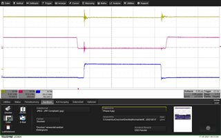
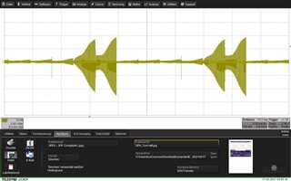
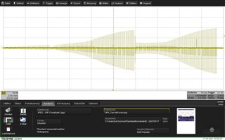
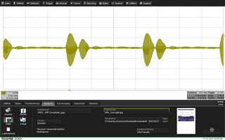
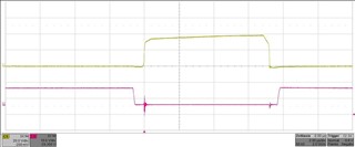
when my customer switches the high side Fet the Gate on the low side fet shows interference. This is also at low IDRIVE values. (Measurement picture below with 30mA IDRIVEP and also low IDRIVEN). With higher IDRIVEP the interference much more bigger.
For the low side FET my customer can increase the IDRIVEP and IDRIVEP and saw no interference by switching..
After layout finished, they were adding a 1µF bypass capacitor between Vin and GND but this did not have any effect.
In layout (pictures available in private session) they realized that the layer under the Vin Pad from the Hide Side FETs is GND potential.
=> Could the issue a capacitive coupling between the Vin and the GND plan under the high side FETs?
=> Any ideas what can be done to reduce the interference?
Thanks
Josef