This thread has been locked.

If you have a related question, please click the "Ask a related question" button in the top right corner. The newly created question will be automatically linked to this question.

DRV8323: DRV8323 gate drive fault

Part Number: DRV8323
Other Parts Discussed in Thread: CSD88599Q5DC

Hi all:

Our products use DRV8323 to drive PMSM.We have often encountered 8323 damage recently,All the damage is  gate drive fault on high-side MOSFET

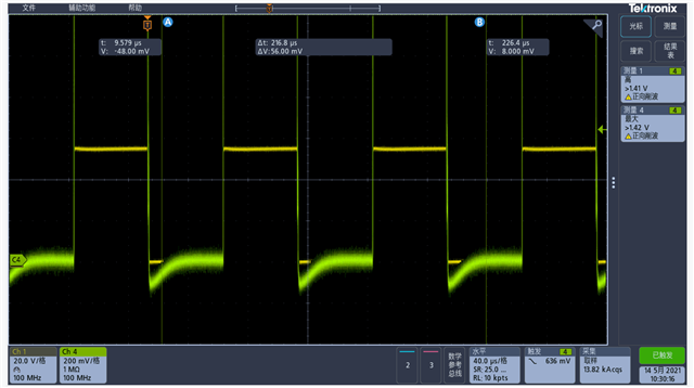
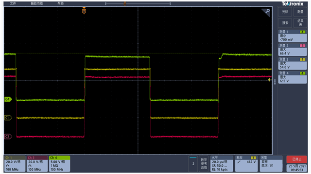
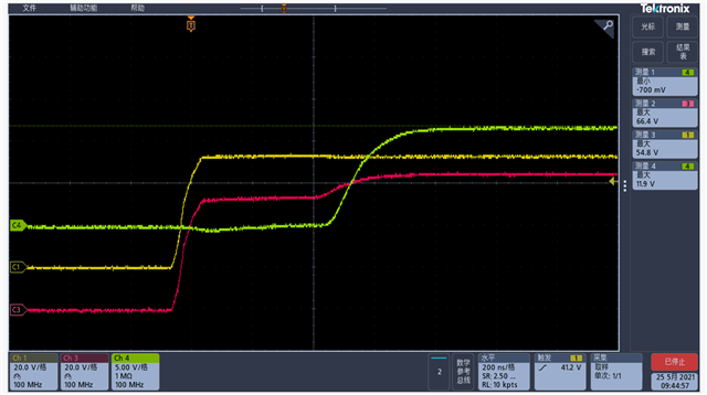
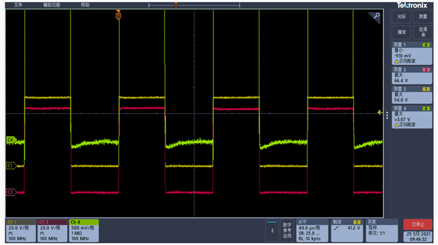
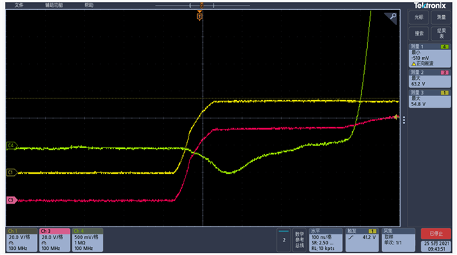
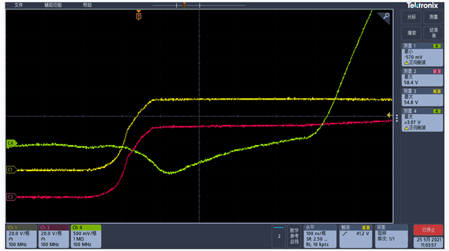
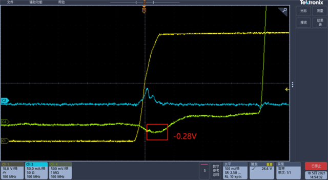
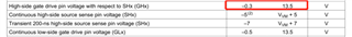
All the damaged devices are DRV8323, not MOSFET. We did some tests and found that the negative voltage of  High-side gate drive pin voltage with respect to SHx(GHx) is out of specification,as shown below

Noted: 

CH1: Continuous high-side source sense pin voltage (SHx) 

CH4:High-side gate drive pin voltage with respect to SHx (GHx)

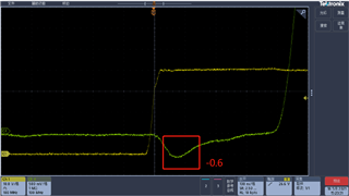
 We found that this negative voltage appears very frequently when the motor has current, which may be the cause of the damage of DRV8323

We use 3x PWM mode ,We tried changing the IDRIVE and dead time, but it didn’t work

Have you ever encountered a similar situation? Do you have any suggestions for this situation?

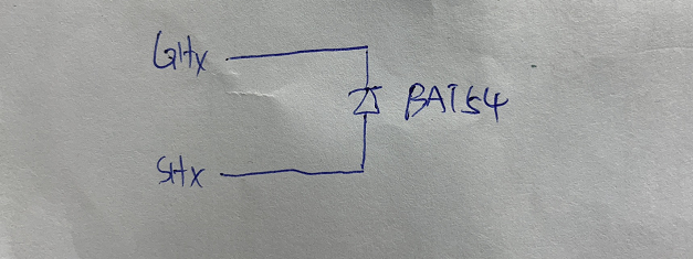
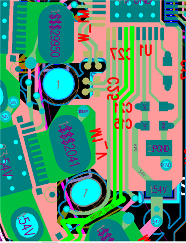
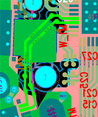
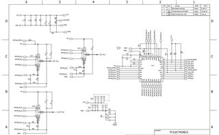
Attach our schematic

Looking forward to your reply

Thanks

ZX

  • Hi X,

    Rise time of output voltage is around 35ns, if output current is a few amps or more it will make pcb layout critical in regard to parasitic inductances. I would adjust IDRIVE settings to increase output voltage rise time to around 200ns and check if DRV8323 works without failure.

    If you can make measurement of output voltage waveform under max. load (with respect to ground plane), I would look for voltage spikes/ringing of frequencies probably around 100MHz close to rising and falling edges.

    In case of that -0.6V, it does violate absolute max. rating but it lasts only 150ns and I think there is little chance it is causing DRV8323 failure though I can not be sure.

    Regards,

    Grzegorz

  • Hi ZX,

    Thank you for posting your question to the Motor Driver forum! 

    We are working on some updates in the datasheet, and -0.6V on the high side gate to source doesn't violate the ratings of the device. 

    1. Are you using a differential probe to measure the high side source to ground voltage? Or are you using a regular single ended probe? The waveform you provided is a bit unusual since it appears that the high side source turns on prior to the high side gate turning on. Could you provide a plot showing the high side gate to ground voltage and the high side source to ground voltage of the same phase? Could you provide one that is zoomed in like the one you provided as well as one more that is more zoomed out that shows several switching events?

    2. What IDRIVE settings have you used in testing?

    3. What is the Qgd of the FET that you are using?

    4. Is channel 1 measurement in reference to ground?

    5. Is the gate fault only occurring on a particular high side phase? Or is it occurring on different phases? 

    6. Does the gate fault usually occur after the driver operating for a while? Or does it occur soon after startup? Once a gate drive fault occurs is the device permanently damaged? or can you clear the fault and try to operate it again?

    If there is significant ringing on the gate and/or source due to high parasitic inductance/ too high IDRIVE settings, this can cause violation of the abs max ratings and can cause damage to those pins. Have you done any resistance measurements on the high side source and high side gate pins to see if there is any damage to those pins when compared to a known good device? If one of these pins get damaged it may cause the gate to not be able to fully turn on, which could trigger a gate fault. 

    Regards,

    Anthony 

  • Hi Anthony,

    1. I'm sure I'm using a differential probe to measure the high side source to ground voltage

    CH1: Continuous high-side source sense pin voltage (SHx) using a regular single ended probe

    CH4:High-side gate drive pin voltage with respect to SHx (GHx) using a differential probe

    CH3: High-side gate drive pin voltage (GHx)  using a differential probe

    2.  The IDRIVE I use normally is :IDRIVEN_HS_1360MA,IDRIVEP_HS_370MA  ,IDRIVEN_LS_1360MA,IDRIVEP_LS_370MA

    I also tested other IDRIVE:IDRIVEN_HS_120MA,IDRIVEP_HS_60MA  ,IDRIVEN_LS_120MA,IDRIVEP_LS_60MA, the waveform is as follow

    3. The Qgd of the FET is 7nC (CSD88599Q5DC )

    4. Channel 1 measurement is in reference to ground

    5. The gate fault is occurring on different phases but all on high side

    6. The gate fault usually occures after the driver operating for a while.

    'The device permanently damaged and clear the fault and try to operate it again', we have encountered both of these situations

    --------------------------------------------------------------------------------------------------------------------------------------------------------------------------------------------

    7. For the beginning of your reply 'We are working on some updates in the datasheet', does this mean -0.6V on the high side gate to source will not damage the device?

  • Hi Anthony,

      Sorry for forgetting thank you for your reply

    During our test ,we found that if we add a clamping diode(BAT54C) between GHx and SHx, there will be a significant improvement

    Do we need to add a diode or just adjust IDRIVE? 

    CH1: Continuous high-side source sense pin voltage (SHx) using a regular single ended probe

    CH2: The current flowing through the diode

    CH4: High-side gate drive pin voltage with respect to SHx (GHx) using a differential probe

    Regards

    ZX

  • Hi Grzegorz,

    Thanks for your reply , I'll try to adjust IDRIVE  

    My question mentioned that the negative voltage still exists after reducing IDRIVE. If the negative voltage will damage the device, do you have any other suggestions?

    Regards

    ZX

  • Hi X,

    Thanks for the waveforms, except that small -0.6V dip I think they look very clean. Would it be possible for you to add waveform of output current of the half-bridge? VM is 54V what is quite close to 65V of DRV8323 max. rating, did you monitor VM during motor braking, there might be an overvoltage if braking energy is not managed properly. It is the only thing that comes to my mind. Maybe analysis of pcb layout would bring some more clues.

    Regards,

    Grzegorz

  • Hi X,

    Does problem occurs with  IDRIVE:IDRIVEN_HS_120MA,IDRIVEP_HS_60MA  ,IDRIVEN_LS_120MA,IDRIVEP_LS_60MA  as well? These IDRIVE  settings are moderate for Qgd = 7nC and should not cause any problems. The waveforms look clean anyway. If adding schottky diodes helps preventing faults then problem probably is related to that negative voltage.

    Regards,

    Grzegorz

  • Hi Grzegorz,

     Pcb layout is as follow, please help analyze if it's not going well

    At present, most of the damage is V phase and W phase

    Regards

    ZX

  • Hi Grzegorz,

    We have now produced 200 machines, but only six are broken. We need to find a reliable solution because repairing is very troublesome.

    Regards

    ZX

  • Hi ZX,

    I can recommend reading TI Application Report  https://www.ti.com/lit/an/slva959a/slva959a.pdf. Traces to C17 could be a bit thicker (lower inductance), trace from VCP to C21 could be thicker as well. C21 and C15 could be placed a bit closer to DRV8323. Another GND via should be placed close to C15. GHC and SHC traces should not form a circle (increased inductance), slightly thinner but shorter and straighter traces may work better. I think pairs GHX and SHX should run close to each other on the same layers (magnetic field cancelling and lower inductance). Ground planes should be as continuous as possible and power bus 54V should be decoupled to ground plane (or to LS mosfet source) at each half-bridge.

    I think that is all what I can say about that layout, the things I mentioned do not guarantee proper working of circuit but make it more probable. I would replace DRV8323 on a few faulty boards and check waveforms on these boards, maybe it would be possible to find something more. If these boards failed again it would proof that something may be wrong with them.

    Regards,

    Grzegorz

  • Hi ZX,

    Anthony will provide his input tomorrow as well.

    Thanks,

    Matt

  • Hi ZX,

    The -0.6V high side gate to source voltage should not cause any damage to the device since it is within the specifications of the datasheet (the updated datasheet will reflect this when it is released).

    The Qgd of the FET you are using is on the low side, so I would recommend reducing the IDRIVE (as Grzegorz mentioned) to around 30mA or 60mA source and 60mA or 120mA sink current and then run the driver for an extended period of time and see if there is no damage. I don't see excessive ringing on the high side gate or source so I am not too confident that the IDRIVE Is the problem, but it is worth trying out. 

    Have you tried to remove a damaged device and put it on a good board to verify that the issue is with the device and not any damaged external components? Can you perform impedance checks on all the high side source to ground and gate to ground pins to see if there is any damage indicated on the pins that is resulting in a lower than expected or higher than expected resistance? This would help give an indication where the event is happening that is damaging the device.

    As Grzegorz mentioned, the gate traces for the FETs look too thin. We recommend a minimum of 20mil gate trace width to minimize parasitic inductance/resistance. This may mean that you start out with a trace as thin as you currently are using, and then once you are far enough from the device to have room, you can increase the width to at least 20 mils. Based on the picture of the layout shown in your previous post, it appears that some of the gate to source signals are shorted together. I am assuming that this was an issue with the image not displaying correctly, but I thought I would mention it.

    Some additional layout tips: Each time a signal goes through a via there will be added inductance to the signal, so it is good to minimize the number of vias used especially in paths such as gate traces. Another thing is you want to minimize the length of traces, especially gate traces, and avoid unnecessary turns or sharp angles. It is a good practice to make turns no more sharp than 45* turns. 

    One thing I would try to avoid is to have the high side gate traces go underneath the switching node of the high side source if the gate traces are on the layer below the switching node. This could cause some coupling from the switching of the source node onto the gate signal. 

    As Grzegorz mentioned, TI's Best Practices for Board Layout of Motor Drivers is a great resource for tips on how to improve your layout. 

    Regards,

    Anthony 

  • Hi Anthony:

    Thanks

     I'll try to use IDRIVEN_120MA,IDRIVEP_60MA and then run the driver for an extended period of time and see if there is no damage

    I tried to remove the damaged device and put a good device on the same board , it can work normally .

    I measured the resistance of each pin to ground of the damaged device . It is no different from a good device

    I will pay attention to the layout on the next batch of products

    Thank you all

    Regards

    ZX

  • Hi ZX,

    Sounds good, feel free to reach out to me if you have any questions on how to improve the layout. 

    Regards,

    Anthony