This thread has been locked.

If you have a related question, please click the "Ask a related question" button in the top right corner. The newly created question will be automatically linked to this question.

DRV8350: Trigger a fault after the power supply joins the common mode inductance

Part Number: DRV8350

Hi Team,

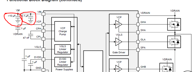
The power supply (PVCC, PGND) of the half-bridge is isolated by the common mode inductor (744220103) to supply power to the DRV8350. 

1. After power on, a fault alarm occurs on the DRV8350nFault pin. Read the fault register value as 0X03FF. After removing the common mode inductance, there is no alarm on the nFault pin, and there is no alarm data on the fault register value.

2. In the same batch of DRV8350, some boards can work normally with common mode inductance (no fault alarm), and some boards cannot work normally with common mode inductance (low nFault output)

Customer would like to know how to prevent DRV8350 from working abnormally after common mode inductance?

Thanks,

Annie

  • Hi Annie,

    Looking at the schematic, is the customer using any bulk capacitance in the circuit? I only see a couple of 4.7uF capacitors on the power supply as well as 2.2uF capacitors on the power stage. If there is no main bulk capacitance then this could possibly cause issues with the power rail. Additionally, it doesn't look like the customer has added the recommended bypass capacitors next to the VM pin (see the image below). I would be curious to see the waveform of the VM voltage at powerup to see if there is any issues there that could be causing the fault issue. 

    One other note, I would recommend that the customer connect all the capacitors on the VM pin on the side of R32 closest to the pin instead of the way it is currently connected (on the side of R32 that is farthest away from the VM pin). This is because It is important to put the bypass capacitors as close as possible to the device, and having a 0 ohm resistor between the VM capacitance and the VM pin will not allow the customer to place the capacitors as close to the pin.

    Regards,

    Anthony Lodi

  • Hi Annie,

    We don't recommend placing a common mode inductor between the driver and the power stage. The inductance in the ground path can cause issues with the ground potential between the driver and the power stage. If the customer would like to achieve more isolation between the analog/digital signals and the power signals, I would recommend that they use a split ground technique instead. This is done by connecting AGND and DGND pins to an analog ground pour, and then the GND pin to the ground pour that is used for the power stage. It is important that these 2 grounds (the analog ground pour and the power stage ground pour) are connected together either with a net tie or a large, 0 ohm resistor to ensure that the potential of these 2 grounds are the same. Also it is important to ensure that both the analog ground and the power stage ground pour has a wide and direct path back to the supply ground. For more information, see section 1 on Grounding Optimization in our Best Practices for Board Layout of Motor Drivers document.

    Regards,

    Anthony Lodi