This thread has been locked.

If you have a related question, please click the "Ask a related question" button in the top right corner. The newly created question will be automatically linked to this question.

DRV8301: DRV8301DCAR

Part Number: DRV8301

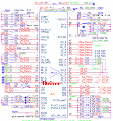
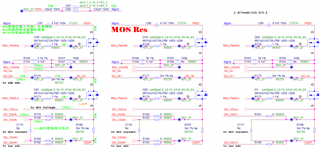
The PVDD1=PVDD2 is 25V or lower.

At first time, the drv8301 seems to work ok at first power up.

The pwm input is ok, and the pwm output is ok. And the Motor is rotating.

But suddenly, the drv8301 seems to damage.

The nFault is always low, (after re-power up or dis/enable the En_Gate )

And the GVDD is low about 2.0V.

The DVDD,AVDD seems to OK.

How can I to do to check the drv8301 is ok or not ?

  • Hi Jianyuan,

    Thanks for posting your question. Since GVDD is in UV, that's why the gate drive outputs are being driven low. 

    Can you provide your schematic for me to review? 

    Thanks,

    Michael

  • i'll provide the spi registers later.

    but it should be point out that the nFault is always low even if re-power up or dis/enable the En_Gate .

    so i think, is it the motor's back pressuse  to increase the voltage of the PVDD1/2 when i use the wrong pwm input.

  • Hi Jianyuan,

    I'll review this and provide some feedback by the end of today.

    Thanks,

    Michael

  • Hi Jianyuan,

    Not sure why RT_CLK is tied to SS_TR and COMP, please see the typical application on the datasheet.

    Recommend using small value resistors for the pull ups for nOCTW, nFAULT and PWRGD. 10k should do the trick. You are also tying these together, please tie them to 3.3 individually.

    It’s best to have a pull up on SDO with a resistor value of ~5k, we typically don’t recommend using just the MCU as a pull up.

    What is the purpose of the 1k ohm resistor on EN GATE and DC_CAL?

    Note that the diode on PH is a shockley diode

    SOx have small resistor values on the application page, you may want to consider adding these to you schematic.

    Which pin is being pulled low, nOCTW or nFAULT?

    Please take a look on page 25 of datasheet and we can go from there.

    Thanks,

    Michael

  • thanks to your timely and constructive reply.

    " ---- Not sure why RT_CLK is tied to SS_TR and COMP... ..."
    these signals are only connect to the Ground "Mgnd"

    " ---- What is the purpose of the 1k ohm resistor on EN GATE and DC_CAL? "
    these signals are only connect to the Ground "Mgnd",
    and i should put the en_gate to low at the power on.
    and the "M3.3v" is the power form the drv8301's buck converter.

    " ---- Which pin is being pulled low, nOCTW or nFAULT? "
    at my bad board, the nFault is low,and the nOCTW is high

    with my bad board, the buck converter is work ok, and the output is 3.3v.
    the DVDD,AVDD ldo output is ok.
    and i think the trickle charge and charge pump is bad.
    and it can get ok after i reworked with a new drv8301 chip.

    because there is something wrong with my spi controller,
    the register will be later.

  • Hey Jianyuam,

    OK, will look at registers next week when you provide them.

    Kind reminder that Monday is a holiday so expect a delayed response.

    Thanks,

    Michael

  • Appreciate your patience and understanding in this matter.

    In my good drv8301 the reg is : ( d10~d0)

     status reg1: 0x00
    status reg2: 0x01
    control reg1: 0x400
    control reg2: 0x08

    In the bad drv8301 the reg is :

    status reg1: 0x600
    status reg2: 0x01
    control reg1: 0x400
    control reg2: 0x08

  • Hi Jianyuam,

    OK so you have two DRV8301, one working on and device, and another that's damaged (GVDD is in UV). Can you spin a motor with good DRV?

    Since the registers are the same, I don't think this is a config issue.

    Can you check the bulk capacitance on PVDDx and make sure the capacitors are not damaged?

    I'd also like you to check the PHx caps and BSTx caps.

    Thanks Jianyuam.

    Regards,

    Michael

  • Yes, i have two DRV8301 board.
    1st, No.1 brd is work ok (the motor is rotating) at Case A.

    2nd, No.1 brd is not work at Case B.

    it’s seam permanent damaged, and the GVDD is 0V.

    and the PVDD current on the device is bigger than normal.

    And it can’t work at Case A apparently .

    3rd, No.2 brd is not work at Case B, and is same to No.1 bard.

           The No.2 brd is damaged also.

           The difference is that the PVDD current of this device is lower than No.1 brd.

           But it’s still bigger than normal case.

    4th, I rework the No.1 brd with a new drv8301,

    The new No.1 brd can work ok (with Case A)

    5th, I read out the register with new No.1 brd(ok) and No.2 brd (not ok)

           And the caps are all ok.


    Thank you very much.

  • Hey Jianyuam,

    I'll get back to you on this by the end of the day.

    Regards,

    Michael

  • Hey Jianyuam,

    Can you please check the layout of the GVDD cap? Check the connection between the device and ground. There should not be any long traces from the device, to the cap, and the finally to ground. Having long traces like that add additional unwanted inductance. 

    I also want you to check the ferites on PVDD1 and PVDD 2.1.

    Thanks,

    Michael

  • thank you for your continued support.

    and i tried to connect the GVDD Caps better,

    but it's still not ok, with the GVDD is still about 1.0v.

  • Hello Jianyuam,

    What happens if you swap the DRV from bad board to good board? I'm trying to find out if the DRV is damaged or if there is a problem with your board. If you can't swap devices, can you try a new device on bad board?

    I see no issues with your schematic. I could take a look at your layout to see if I see any issues with it if you'd like.

    Try to take a close look at each board, working board vs not working. Do you notice any differences? Bulged electrolytic caps indicate that they are damaged, I'm not sure if you're using these.

    We have a layout best practices guide I'll link here that you could take a look at. 

    https://e2e.ti.com/support/motor-drivers-group/motor-drivers/f/motor-drivers-forum/746299/faq-best-practices-for-pcb-layout-of-motor-drives

    Regards,

    Michael

  • Hey Jianyuam,

    Is there any additional assistance I can provide on this case? Were you able to figure out why GVDD was not outputting the correct voltage? 

    Regards,

    Michael

  • I think the drv8301 is damaged . as mentioned earlier, the board can work ok after rework with a new drv8301.

    My “wrong” pwm will generate the back pressure voltage at the PVDD-1 -2, and it exceeds 65V.

  • I think the over-voltage PVDD damaged the Trickle Charge and Charge Pump circuit .

  • Hey Jianyuam,

    Yes PVDD will likely be damaged if it gets exposed to more than 65V, since that is the ABS max of PVDD. Even operating at 60V, (which the max recommended operating DC voltage) there could be transients that could swing PVDD above 65V and damage the device. 

    Is it possible for you to operate at a lower voltage? I see that you are able to swap the DRV8301 and then your board worked fine. However if the PVDD pin gets exposed to this high voltage, the problem will happen again. I think the root cause of the DRV failing is that you're operating very close to ABS max voltage on PVDD.

    Let me know if you have success spinning a motor once you bump down the voltage (if that's possible in your application).

    Regards,

    Michael


  • Yes, after I optimized the PWM timing, the motor drive has been working normally so far.

  • OK I'm glad you were able to resolve this. Feel free to click  "ask a related question" if you need any additional help. I'm going to closed this thread for now.

    Regards,

    Michael