This thread has been locked.

If you have a related question, please click the "Ask a related question" button in the top right corner. The newly created question will be automatically linked to this question.

DRV10983: Standby version performs similar to Sleep version

Part Number: DRV10983

Hi E2E,

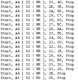
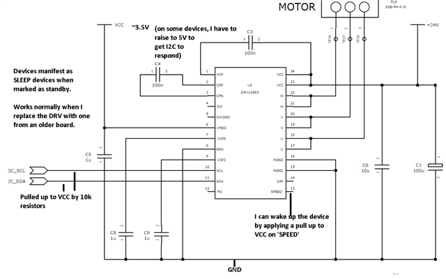
Our customer is using the DRV10983PWP and it was observed that the device is behaving like DRV10983Z (sleep mode version) and requires a 5V core voltage before the I2C will work, and then any reads result in 0x00. The Vreg is supplied by an external buck regulator (~3.48v). The device enters sleep mode and the customer wakes them up with a 3v3 pull up on pin 13. Please advise why the device has this behavior.

Regards,
Carlo

  • Hey Carlo,

    What do you mean by 5V core voltage? Is this the supply voltage?

    If you are trying to read from the registers while the device is in sleep or standby mode, you will read 0x00. When the device is in sleep or standby, you will only be able to read the EEPROM settings. Once you wake the device up by forcing 3.3V on the speed pin, the device will wake up and you will be able to read from any register. 

    Can you share the schematic? 

    Thanks,

    Michael

  • Hello Michael,

    You are correct, the 5V is the supply voltage. They have put an older parts into their boards from another DRV10983 batch and it works fine. According to the cutsomer, in their design vreg pin is supplied by an external regulator set to ~3.5V. For the majority of my devices, this sufficient to power the internal logic and once they pull up the speed pin, everything works. 

    For some devices, they have to provide 5V to vreg before the device communicate via I2C. The customer have to remove the pull up resistors on board (as the I2C on the DRV10983 is not 5V tolerant). They use an off board arduino Nano, with 4k7 pullups to 3v3 then link the grounds. This is sufficient to allow I2C writes, however the reads return as zero.They've try pulling up the speed pin when attempting to setup the eeprom to see if this allows reads. However one of the config registers write is supposed to set up the Vreg supply voltage to 3.3V and the device still requires 5V after an apparently successful write.

    Based on the customer, this device was bought as a replacement for the current ones that appear to be malfunctioning. Would it be possible  to qualify these by batch number since the older parts works after swapping in their design?

    Here is the image of the device.

    Regards,
    Carlo

  • Hi Carlo,

    The VREG pin is a power output pin. This means you do not want to force voltage onto this pin. When the device is nominally powered up the VREG will output either 5V or 3.3V depending on how VREGSEL is set. 

    Forcing voltage onto this pin could cause internal damage to the device depending on how much current flows into the pin. 

    Please share the customers schematic. Without this it's hard to help you debug further.  

    Thanks,

    Michael

  • Hello Michael,

    Here is the response I received from our customer:

    Looking at your datasheet, SW is the switching output, and VReg is used to power the internal circuits/provide feedback ie it is an output to the internals of the device but is defined as a power pin. It powers the 3.3v LDO and 1.8v LDO. if it didn’t, how would the internal buck regulator be able power the internals as it needs external components? anyway, this is a proven circuit. Which works when I switch the device to one from an older batch.

    Plus I’d be very surprised if I damaged the device in a way which would convert these to sleep mode devices!

    Also let me point you to this: e2e.ti.com/.../drv10983-powering-vreg-from-an-external-source

    Here is the schematic for your reference.


    Regards,
    Carlo

  • Hi Carlo,

    We will reach out to you over email.

    Thanks,

    Matt

  • Hi Carlo,

    I am going to close this thread as per our email conversation. Let us know if you need any other help!

    Thanks,

    Matt