Other Parts Discussed in Thread: DRV8301
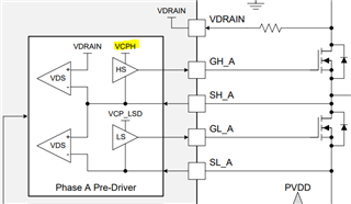
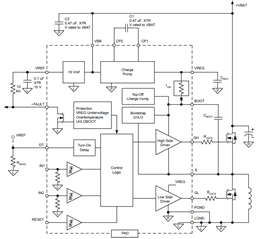
I just found the charge pump output VCPH pin should be connected to the PVDD pin using a 2.2 μf capacitor, rather than to the SHA pin (Source pin of high side MOSFET).
And I have two questions about it:
1) The reference gound of charge pump output (VCPH) is PVDD?
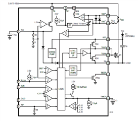
2)I also found the charge pump was usually connected to the source pin of high side MOSFET from other high side gate driver datasheet shown as FIG.2. What's the differences between two patterns?
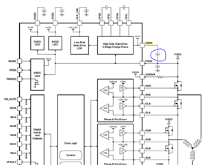
Fig.1
Fig.2