This thread has been locked.

If you have a related question, please click the "Ask a related question" button in the top right corner. The newly created question will be automatically linked to this question.

DRV8353RH-EVM: DRV8353RH-EVM

Part Number: DRV8353RH-EVM
Other Parts Discussed in Thread: DRV8353R, DRV8350

Good morning,

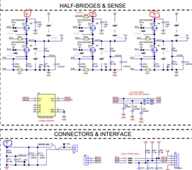
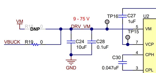
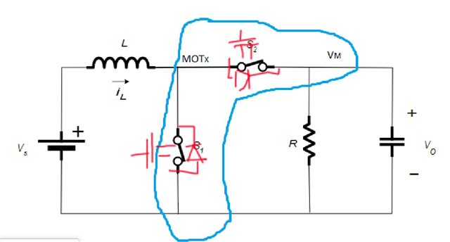
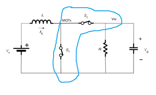
I have a DRV8353RH-EVM which I intend to use as converters/inverters. The fact is that we bought this to use it in the split rail mode. However, I am not sure how this works exactly. When working as a boost converter, we use just use one half bridge of the EVM in the way the attached picture shows (boost converter topology); the encircled region is part of the EVM, the rest is connected from the outside.I understand that in the split rail configuration we can have V0 (attached picture) different to the voltage connected in J5. Is this possible?  If I am wrong, I really hope you can explain a bit more this split rail configuration.

Thanks in advance,

Jon

  • Hi Jon,

    Vo will have to be VDRAIN, since that is the voltage at the high-side MOSFET (S2) drain. The VM pin can be a different voltage than VDRAIN, for example Vs, as long as it is in the operating range of the DRV8353R.

    VDRAIN is connected to J5 through the fuse on the board. The VM pin is not actually connected to J5 or VDRAIN by default.

    The default configuration of the VM pin is powered by the buck regulator through R19. You can always remove R19 and tie your own voltage on TP16.

    Thanks,

    Matt

  • Hi Matt,

    Firstly, thanks for your answer. However, I am a little confused. I guess I am wrong, but looking at the schematic of the EVM, we see that the high side MOSFET is connected to the VM node, isn't it? And the J5 connection is also connected to VM.

    I cannot attach a picture of the schematic, I don't know why.

  • I just attached the picture. Are you suggesting that the red encircled VM and blue encircled VM are different? Thanks in advance,

    Jon

  • Hi Jon,

    The naming convention on this EVM is quite confusing and not ideal. You can see that the VM pin isn't actually tied to the VM node.

    Thanks,

    Matt

  • Hi Matt,

    I have a doubt. Notice, that when using the half bridge as a boost converter (I sent the topology previously) at the initial moment, we have null voltage in VDRAIN (or above top MOSFET in the half bridge). Therefore, VM cannot be possitive as the internal Buck regulator has no input voltage. In this situation, how can I feed VM independently from the outside?

    Thanks in advance,

    Jon

  • Hi Jon,

    The high-side MOSFET body diode saves us for the start-up condition. The MOSFET drain will be charged from the input voltage through the inductor and high-side MOSFET body diode.

    It may be easier to simply remove R19 from the board and supply an external voltage onto TP16 (VM pin). Since the buck input voltage will vary with the boost output voltage, it may be a little complicated.

    Thanks,

    Matt

  • Hi Matt,

    Thank you very much for the answer you provided. However, I have another question regarding to the Hall sensing. I am using the 6xPWM mode and need no hall detection at all. Therefore, in my application, has J3 any utility? Could I safely remove the J3 and the potentiometer from the board?

    Thank you in advance,

    Jon

  • Hi Jon,

    Yes, you can remove J3 and the potentiometer from the board. They do not have any purpose in 6x PWM mode.

    Thanks,

    Matt

  • Hi Matt,

    And could we use the J3 for other purposes? Looking at the schematic it seems obvious that if we take out the resistances and capacitors in the pciture attached we have three isolated nodes in J3. However, what happens with 3.3V and GND? are they connected from the board or they appear in the schematic because we are supposed to connect 3.3V and a ground there? Thanks in advance,

    Jon

  • Hi Jon,

    From the schematic you can see that GND and 3.3V are hard wired to pins 1 and 5 of J3. Pins 2-4 are not connected to the DRV8350 by default due to the resistors (R48, R50, R52) being DNP. HALLA, HALLB, and HALLC are tied to the launchpad headers. 3.3V is generated from LDO U3 on the board from the buck output.

    Thanks,

    Matt

  • Hi Jon,

    Do you need any further help on this thread?

    Thanks,

    Matt