This thread has been locked.

If you have a related question, please click the "Ask a related question" button in the top right corner. The newly created question will be automatically linked to this question.

DRV8353R: Gate slew rate disturbed when switching load

Part Number: DRV8353R
Other Parts Discussed in Thread: DRV8301, DRV8353, MOTORWARE, CSD18533Q5A

Hello,

I swapped DRV8301 with DRV8353 on a already working design but I obviously have issues with the gate drive control.

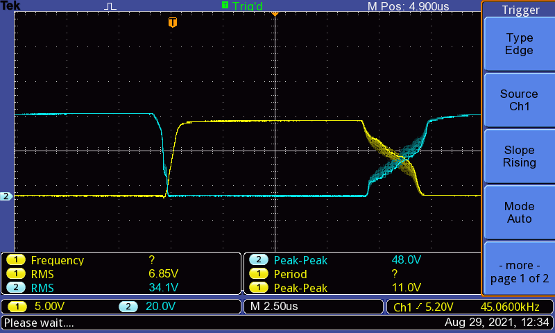
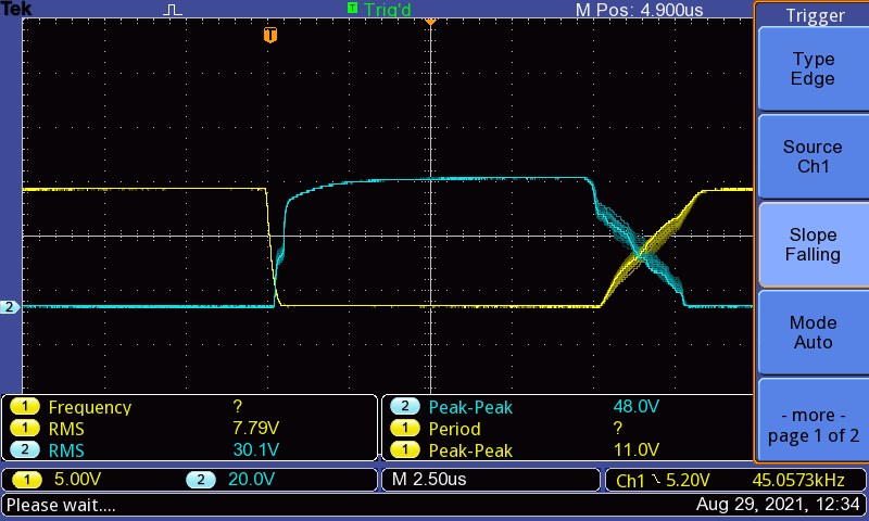
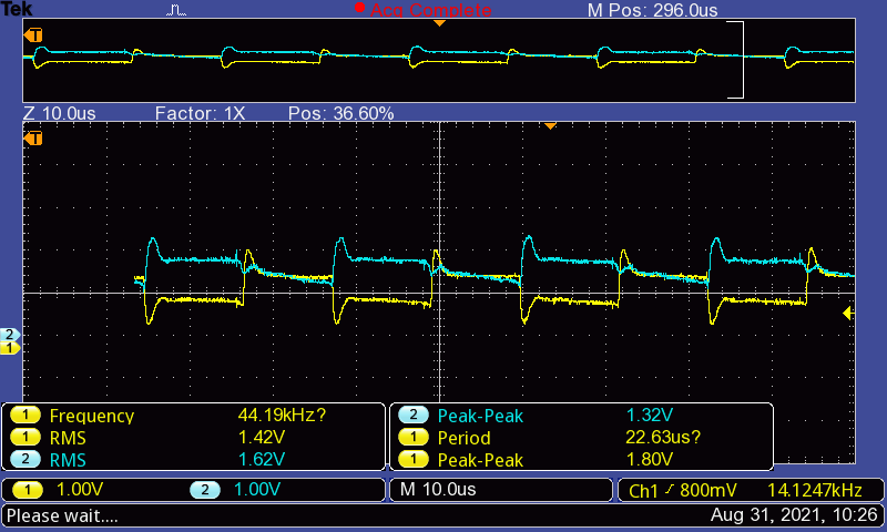
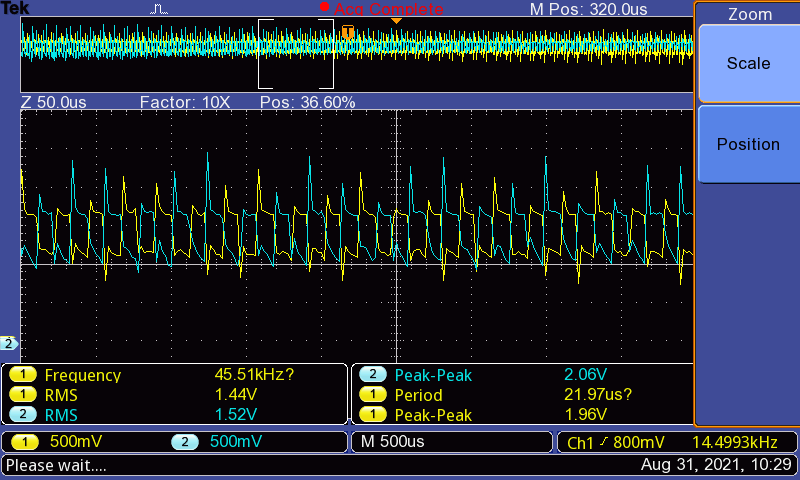
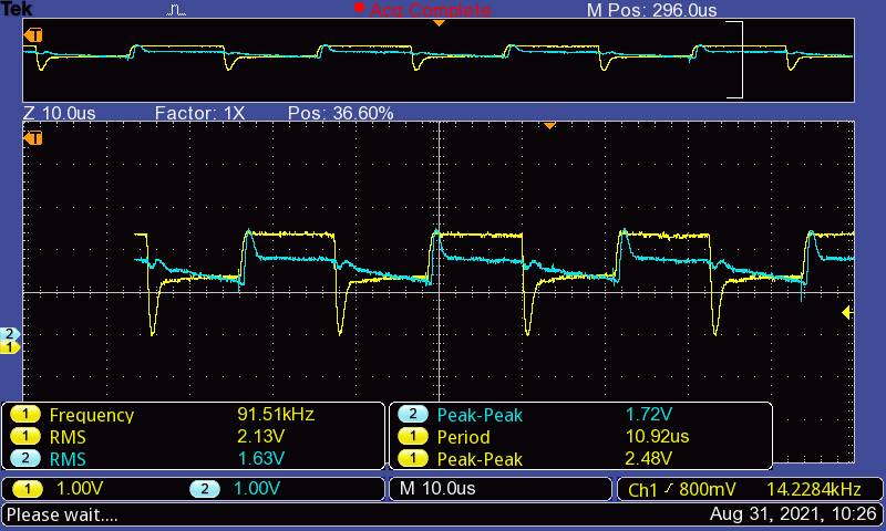
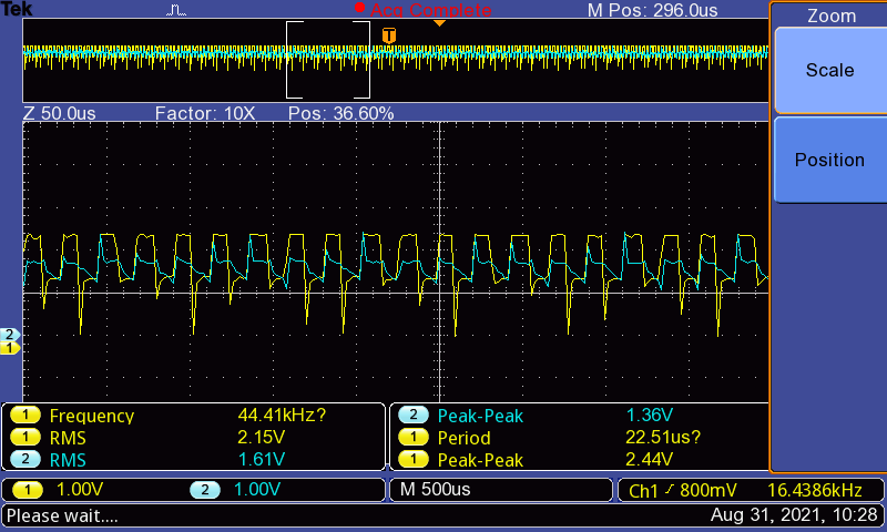
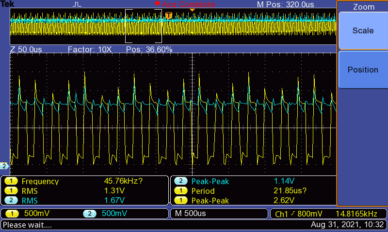
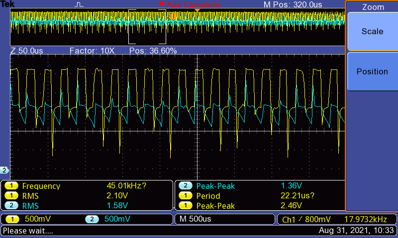
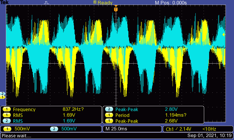
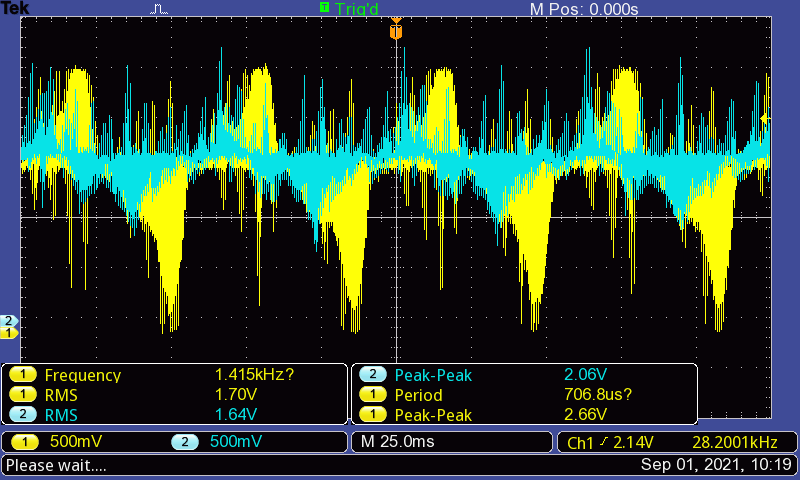
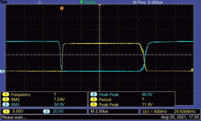
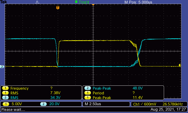
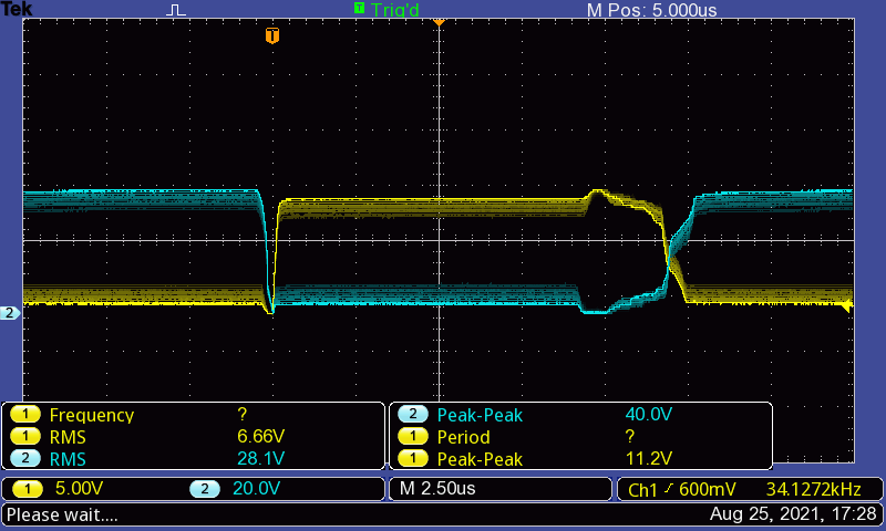
I run motorware lab 1c which is for closed loop current control and this is what I see on the scope:

0 Amps applied (Iqref_A parameter)

0.5 Amps applied

1.0 Amps applied

2.0 Amps applied

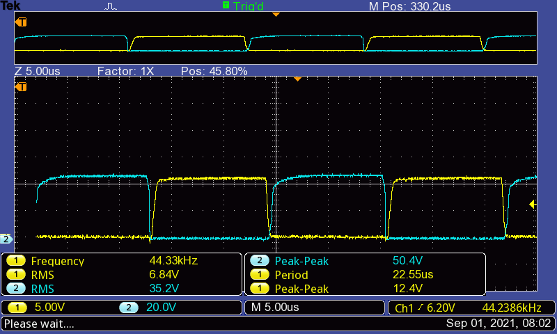
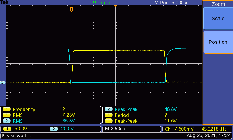
So the scope gave me the finger Slight smile

If I put more current, the OCP protection cuts out the driver.

Please advice on what could be wrong in this situation. In the previous design I have a gate resistor because the previous driver didn't had slew rate control. Here I'm using the following settings:

IdriveN: 200mA and IdriveP: 150mA

  • Hi Georgi,

    Can you please provide your schematic (including power stage) ? You may need to lower the IDRIVE on DRV8353 even more depending on the FET you're using. It seems like you're turning the FET on too hard, which is a result of too high of an IDRIVE. 

    Thanks,

    Michael

  • Hi Michael,

    Thanks for answering. I'll try lower settings. I'm using CSD18533Q5A FETs 

    Regarding the schematic - I've requested friendship so I can PM you them.

  • Those FETS have a Qgd of 5.4nC. You can calculate the rise time of these FETS by dividing the Qgd by the IDRIVE setting you're using.

    So 5.4E-9/150E-3 = 36ns (too fast). We recommend our customers design the system such that the rise time is between 100-200ns. The min IDRIVE you can choose for DRV8353 is 50mA, without using a series resistor. If you select this IDRIVE setting, then I expect you to have a rise time of ~108ns. Can you give this a try?

    Thanks,

    Michael

  • I did this calculation, but thought that the driver will manage that speed.

    So, I lowered the Idrive P and N to 100mA and 50mA, but that was not enough and the scope showed similar results. Do you suggest that I must use gate resistors and lower the times even further? Unfortunately, when I swapped the driver I removed the gate resistors from the PCB and probably I should experiment with some "less fancy" FETs. Do you think the gate drive current is the problem here? BTW, I've PM-ed you the schematic.

  • Hi Georgi,

    I don't see anything wrong with your schematic, it looks good and similar to our EVM. I believe the root cause of your issue is due to ground bouncing, however I can't say for sure without reviewing your layout. Can you send me your layout so I can verify?

    Regards,

    Michael

  • Hi Michael,

    I PM-ed the layout. I'll review the grounds together with you. I'll be surprised, because similar layout is already working for me with the other driver.

    Best,
    Georgi

  • Thanks Georgi,

    I will review it and provide feedback as soon as possible.

  • Hi Georgi,

    I've had time to review your layout. The main issue I want to highlight is that you are using thermal reliefs for several of your components (sense resistor, bulk caps, kelvin connections for CSA). Using thermal reliefs for high current applications is not recommended as all the current will have to flow over a smaller area vs if you were using direct connection. In most motor drive applications we would like to see a direct connection. Some PCB software's will default to thermal relief, so if you change these I think your problem will -hopefully- be resolved.

    Second I recommend moving your sense resistor to the same plane as your MOSFETS (top layer). If you have you sense resistor on another plane than the MOSFETS, then the signal will have to pass through vias and this adds lots of additional inductance. 

    Thanks,

    Michael

  • Hi Michael,

    Absolutely valid point! Thanks for the advice. Thermal reliefs are on for those components and this will prevent high current to flow through them. I must have been in a hurry, because I have no previous design with thermals on that place :) I put some wires in place to avoid thermals, but things didn't improve much. I noticed something and this must be the way I'm measuring with the scope. See the following oscillograms:

    This is the same experiment, just the slope of the trigger is changed. To me, it is obvious that the scope is capturing it wrong. I'm using 10x low inductance voltage probe and BW filters are off. I should say the scope is picking up some noise, but then I change the slope - it's the opposite signal change that is affected. On the other side this is observed only when current is applied to the FETs... so a bit clueless here.

  • Ok, I changed the scope settings. I was acquiring the signal wrongly by averaging the samples. Now I switched back to single samples and they are perfect. The displayed oscillograms look like this because the driver is constantly modifying the gate pulses in order to fine control the FETs. So please ignore them.

    Now I sampled in the software the following:

    I_data[0] = _IQmpy(gAdcData.I.value[0], _IQ(USER_IQ_FULL_SCALE_CURRENT_A));

    I_data[1] = _IQmpy(gAdcData.I.value[1], _IQ(USER_IQ_FULL_SCALE_CURRENT_A));

    I_data[2] = _IQmpy(gAdcData.I.value[2], _IQ(USER_IQ_FULL_SCALE_CURRENT_A));

    And on the graph I can clearly see the difference in current measurements. I set the Iqref_A to 0.2A which must be the phase currents. Now the phase B is only correct as it shows -0.2 to 0.2 on the graphs. Phase C reads -0.1 to 0.1 and phase A reads -1.0 to 1.0. So I conclude that the phase current measurements must be wrong, but why?

  • Hey Georgi,

    A quick note.

    When setting up a trigger on a scope, it's best to choose the trigger to be somewhere around the middle of the waveform. So if a waveform is swinging from 0-12V, a 5-7V trigger is appropriate. In your first plots I see you were triggering around 600mV. Triggering at a low voltage like this could result in false triggers due to noise. I see that you changed your voltage trigger to 5.2V, awesome. You could also increase the resolution of these waveforms so they take up the entire scope screen. When capturing waveforms like this we want to maximize the entirety of the scopes screen. 

    Back to the problem at hand:

    I don't know if placing wires over these thermals to 'connect them', will be sufficient. Can you show me a picture of the board so I can get a better understanding? Also the placement of the sense resistor on a different plane is the other main issue.

    This likely will require a board redesign, you may be able to blue wire your way to victory, it's worth a shot.

    And on the graph I can clearly see the difference in current measurements. I set the Iqref_A to 0.2A which must be the phase currents. Now the phase B is only correct as it shows -0.2 to 0.2 on the graphs. Phase C reads -0.1 to 0.1 and phase A reads -1.0 to 1.0. So I conclude that the phase current measurements must be wrong, but why?

    Can you share this plot/waveform please?

    Thanks,

    Michael

  • Hello,

    Yes, I'll produce a new scope of the gate voltage to confirm that the mentioned above scopes are invalid.

    Apart from that - I examined the phase currents and I observed something. Again, the motor is in voltage control (lab1b) and during the rotation I captured different events:

    A period with normal phase currents (SOB is blue and SOC is yellow):

    A period with irregular SOC current. Looks like is saturated:

    Seems like the SOC phase current is measuring much more current than the SOB current channel (SOA is similar to SOB)

    FETs seems to be working ok. The motor is spinning normally for this control mode. Do you think those current measurements are ok?

    Best,

    Georgi

  • I did some more scopes. So currently I conclude that the phase C current reads lower than the other ones. To eliminate any potential internal issues with the driver I replaced it and also replaced the shunt resistors and the capacitors. The scope read the same lower current. I also read lower peak-to-peak voltage on the sense_p and sense_n pins of the driver of the C phase compared to the other ones. Swapped two phases of the motor also to eliminate potential issues with the windings. If that was due to bad layout the shunt must have read higher current instead of lower because of a potential higher voltage drop. Do you have any thoughts?

    Here are phase A and phase B

    But here are the phase C (blue probe) and phase B currents

    And BTW here are the gate voltages without the applied accumulation. Looks pretty fine to me

    Best,

    Georgi

  • Hi Georgi,

    I will get back to you on this by the end of the day.

    Thanks

  • Hey Georgi,

    The current waveforms you provided do not look normal, same for the SOx signals.

    After talking to other team members, we believe that the board will  need a re-design to change the thermal reliefs to direct connection and to move the sense resistor to the same layer as the FETS. Blue wiring all of these thermal reliefs is adding a significant amount of inductance and this will effect the whole system. The gate drive traces that you have are also pretty small, so I'd recommend widening those in your next revision. 

    I'm linking you to two app notes, one covers system design consideration for high powered motor applications, and the other is a best practices for PCB layout for motor drivers.

    I look forward to seeing your next revision of the board.

    Regards,

    Michael

  • Ok Michael,

    Understood. I'll redesign, but still I feel the current is too small to be affected by the thermals at this point. Speaking of 1-2 Amps. I'll order a new design from the PCB house immediately but meanwhile I'll experiment with this one moving to lower currents. Thanks for the suggestions and all the support!

    Best,

    Georgi

  • I'll look this over with one more team member & see if there's anything they would like to add, let me get back to you on this once more tomorrow. Thanks Georgi.

  • Sure, thank you for your efforts. Meanwhile I consulted a colleague and decided to put some big resistors in order to replace the motor with a more simple resistive load in order to plug some PWM values and check the current feedback. Swapped all the MOSFETs, shunt resistors, capacitors and motor phases in order to eliminate any potential issue with the motor or any of the components mentioned - the result was the same. The experiment with the resistive load is not done yet.

    Best,

    Georgi

  • Hi Georgi,

    OK let me know results once you try a resistive load, although I don't expect the results to be different. 
    What you could do instead of blue wiring the thermal reliefs (which is how your setup is now right?) is use an exacto-knife and cut the thermal reliefs such that it makes a direct connection. You would have to solder these junction points too to make an electrical connection.    

    On the current waveforms you provided there is a lot of added inductance which is causing they waveforms to look as they do. I'd expect the output of SOx to be around 2V, which is what we see on SOA and SOB. I don't think this is a result of the MOSFETS you're using or the caps. 

    Regards,

    Michael

  • Hello Georgi,

    Do you have any additional feedback on this thread?

    Thanks,

    Matt

  • Hello Matt,

    Just received my redesigned board. At first test seems that the wrong current measurement is similar to the previous layout but I'll need a little bit more time to investigate. I'll get back to you once I collect more data.

    Best,

    Georgi

  • Hi Georgi,

    Sounds good, please keep us in the loop!

    Thanks,

    Matt