This thread has been locked.

If you have a related question, please click the "Ask a related question" button in the top right corner. The newly created question will be automatically linked to this question.

DRV8320R: design and brakes questions

Part Number: DRV8320R
Other Parts Discussed in Thread: TMS320F280049C, DRV8316, LAUNCHXL-F280049C, , DRV8316REVM, DRV8320

Hi Team,

My customer is surveying our DRV8320R, below are some questions need you reply! 

  1. Does DRV8320R must need Hall sensor to determine rotor position for drive ?
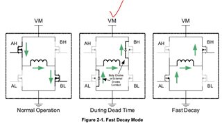
  2. Does DRV8320R feature fast / slow / mixed decay recirculation mode during the braking ?
  3. When DRV8320RS brakes, how's the BEMF (back EMF) impact the circuit? Should add any protection or not?
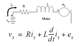
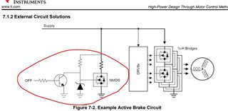
  4. When DRV8320RS brakes, the energy in motor go through like below right ? How customer judge need to add a Active Brake Circuit or not in their design ?

Thank you!

Kai

  • Hello Kai,

    DRV8320R does not integrate the commutation and control of the motor, unless you are using 1xPWM control (trapezoidal) with Hall Sensor feedback.

    The most common use of DRV8320R is along side an MCU which is executing the motor control algorithm. In 6xPWM and 3xPWM modes, the DRV8320R can be operated in fast, slow, or mixed decay as controlled by the MCU through the PWM inputs.

    Thanks,

    Matt

  • Hi Matt,

    Thanks for your reply.

    So which mean DRV8320R is just a pure 3 phase gate motor driver, customer need to implement the motor control and fast, slow, or mixed decay control by themselves right ?


  • Hello Kai,

    That is correct.

    What motor type is the customer using, and what is the voltage and current requirement?

    Thanks,

    Matt

  • Hi Matt,

    Customer is designing a 24V / 110W motor.

    There would like to know

    1. If they implement either fast, slow, or mixed decay control in the MCU, do they still need another protect schematic like below in design ?
    2. How customer judge they need to add a Active Brake Circuit or not in their design ?
    3. Can we provide any equation or reference design which had the resistance value, MOSFET part number for customer reference ?
      Since they would like to know how to design this schematic include resistance value and MOSFET part choose.
    4. Can we provide fast, slow, or mixed decay control source code to customer ?

    Thank you!

    Kai

  • Hello Kai,

    1. An external active brake circuit is not necessary in many designs, especially low-power motors. These circuits become very important in high power systems or systems that do not have much bulk capacitance. If the motor can act as a generator by being externally forced, this may indicate the need for an active braking circuit to dissipate the generated power. 
    2. At the customer voltage and power, I would not expect the customer to need to implement such a circuit.
    3. On this circuit, the zener clamp needs to have a breakdown voltage below the abs max rating of the system so that the NMOS can begin to turn ON before the voltage ratings are violated. The MOSFET needs to have a VDS rating of the highest supply voltage in the system and be able to dissipate the required power.
    4. In a BLDC motor, fast decay occurs when all MOSFETs are OFF (INHx and INLx are all low) while slow decay (brake) occurs when all INLx are high (low-side brake) or all INHx are high (high-side brake). FYI - mixed decay is a term mostly used in stepper motors, not BLDC.

    Thanks,

    Matt

  • Hi Matt,

    If customer is designing a E-bike, which mean the motor can act as a generator, will need external active brake circuit ?

    Kai

  • hello Matt,

    I'm Kai Shen, the customer of Kai Lai, using DRV8320RS to drive 24V / 110W BLDC, the schematic used refering EVM (www.ti.com/.../BOOSTXL-DRV8320RS)).


    I want to achieve brake mechanism,

    in hardware, should I add or modify any schematic or notice something else?

    in software, besides "fast decay occurs when all MOSFETs are OFF (INHx and INLx are all low) while slow decay (brake) occurs when all INLx are high (low-side brake) or all INHx are high (high-side brake)", any coding should i noitce?


    thanks.

    Kai Shen

  • Hi Kai,

    Nice to meet you.

    At the motor power that the customer is stating, I do not expect that a brake circuit will be needed. However if the motor energy is not allowed to re-charge the battery, it may be required. The motor-generated energy has to go somewhere.

    Commanding a fast decay (coast) or slow-decay (brake) is done by configuring the PWM controls to the DRV8320R as I noted above. The MCU will need to be controlling the motor with a sensored control scheme (trap or FOC).

    Thanks,

    Matt

  • Hi Matt, 

    Thanks for your reply, i still worry about the motor, driving circuit and battery, 

    1. Beside experience, how we estimate need a brake circuit or not? is any guidance?

    2. Is formula to calculate the BEMF and current when brake no matter fast decay or slow decay?

    Thanks, 

    Kai Shen

  • Hello Kai,

    1. If the motor is capable of generating a higher voltage than the supply when being externally spun, that means it may be necessary to implement an external brake circuit. You can check the back-EMF constant and maximum speed that the motor will spin when not being driven.

    2. Use the back-EMF constant to calculate the back-EMF voltage generated when the motor is spinning. The torque constant can be used to calculate how much current the motor can generate.

    Thanks,

    Matt

  • Hi Matt, 

    In the article, The art of stopping a motor – VM pumping (e2e.ti.com/.../art-of-stopping-the-motor-vm-pumping), mention that the VM pumping mechanism (back-EMF may greater the supply voltage), it's can't corresponding the formula you provide, what's the correct formula when braking?

    Thanks, 

    Kai

  • Hello Kai,

    This article has a general guidance on the amount of supply pumping that we see across motor types. This is just an estimate.

    Thanks,

    Matt

  • Hello Matt,

    May I make a brief summary as below?

    1. I have no externally spun, means that i don't worry the VM pumping (generating a higher voltage than the supply), no matter the other motor condition (ex. motor type, motor power, motor parameter)? it also means the back-EMF won't greater the supply voltage.

    2. The motor always can bear the the current when braking

    Thanks,
    Kai Shen

  • Hello Kai,

    That is correct, if there is no mechanism to spin the motor, the back-EMF will never be larger than the supply voltage. However, if you suddenly disconnect the power supply and coast the motor, it will generate some voltage & current as it spins down.

    When braking the motor, current will not pump the supply and is dissipated in the motor and MOSFETs.

    Thanks,

    Matt

  • Hello Matt,

    Got it, if there is no mechanism to spin the motor, I have no need to worry the motor will be broken when braking. Thank you very much. 

    About the MOSFETs, how should I estimate the MOSFETs can bear the braking process?

    Thanks,
    Kai Shen

  • Hello Kai,

    During braking, almost all of the motor mechanical energy is converted into current. Make sure that this will not exceed the current ratings of the MOSFETs or damage the motor itself.

    Thanks,

    Matt

  • Hello Matt,

    For motor, as mentioned before, "the torque constant can be used to calculate how much current the motor can generate".

    Since the motor can be driven, means that the torque is under rating, so the current when braking is always under rating, is any other factor I need to take consideration?

    Thanks,
    Kai Shen

  • Hello Kai,

    When you assert a brake, the motor will generate higher current than the torque constant indicates. This is because the motor back-EMF is shorted and this can result in the current rapidly increasing before slowly decreasing.

    Thanks,

    Matt

  • Hello Matt, 

    So .. how to calculate the current when I assert a brake?

    Thanks,

    Kai Shen

  • Hello Kai,

    You may be able to estimate this current by calculating the mechanical energy (rotational energy) of the motor (1/2*I*w^2) and converting it into electrical energy or current (1/2*L*I^2). This may be a difficult calculation to run because you may not know the motor's moment of inertia. 

    You can determine this value experimentally by braking the motor while it is operating at maximum speed. You can start by braking for a short time (1 ms) and then go to coast while measuring the motor current on an oscilloscope to see the peak current. Slowly increase the brake time as you observe the motor current to ensure that you do not damage the motor.

    For your motor, it is possible that asserting a full brake is OK for it. The above procedure allows you to experimentally see what the brake current will be.

    Thanks,

    Matt

  • Hello Matt, 

    1. As you previous mentioned "Commanding a fast decay (coast) or slow-decay (brake) is done by configuring the PWM controls to the DRV8320R", this command can't control the braking time as I know, so how could I know the braking time exactly? any reference (like formula or document). 

    2. I have parameters of 2 motors as below, after calculating, the EVM of DRV8320RS (www.ti.com/.../BOOSTXL-DRV8320RS) can't bear the current and power, so I still need to add an external active brake circuit? or I miss something? 

    24V / 110W
    Rated speed: 2800 RPM ( = 294 rad / sec)
    No load speed: 3600 RPM
    Rate Torque: 3.77 kg-cm
    Rate Current: 6.5 A
    Peak Torque: 13.66 kg-cm
    Peak Current: 25.3 A
    Resistance: 0.44 ohm
    Inductance: 0.83 mH
    Inertia: 500 g-cm2 (= 0.00005 kg-m2)
    --

    [Motor2]
    48V / 400W
    Rated speed: 3000 RPM ( = 315 rad / sec)
    No load speed: 6409 RPM
    Rate Torque: 12.95 kg-cm
    Rate Current: 11.8 A
    Peak Torque: 38.84 kg-cm
    Peak Current: 35.4 A
    Resistance: 0.18 ohm
    Inductance: 0.61 mH
    Inertia: 280 g-cm2 (= 0.000028 kg-m2)
    --

    use formula (1/2*I*w^2),
    get the mechanical energy (rotational energy) is 2.16J for Motor1
    get the mechanical energy (rotational energy) is 1.39J for Motor2
    --

    use formula (1/2*I*w^2) = (1/2*L*I^2),
    get the current is 102.05A for Motor1
    get the current is 95.44A for Motor2
    --

    if the braking time is 1ms,
    get the power is 2160W for Motor1
    get the power is 6270W for Motor2
    --

    Thanks, 

    Kai

  • Hello Kai,

    That EVM uses CSD88599 MOSFETs which are rated up to 60V & 400A pulsed current. It sounds like the components on the EVM can withstand the potential high current when braking the motor. The large blue headers to the motor are the primary factor to limit the current rating of the EVM, so you may consider removing those and soldering directly onto the EVM. You will likely need to confirm that the motor itself will be OK. 

    Bear in mind this is a first-order calculation. In reality, the current will probably be lower due to the motor resistance - this is why it is best to run an experiment to verify the actual braking current.

    Thanks,

    Matt

  • Hello Matt,

    1. About the braking time, As you previous mentioned "Commanding a fast decay (coast) or slow-decay (brake) is done by configuring the PWM controls to the DRV8320R", this command can't control the braking time as I know, so how could I know the braking time exactly? any reference (like formula or document).

    2. "CSD88599 MOSFETs which are rated up to 60V & 400A pulsed current", the pulse is below 0.1ms, is figure SOA (safe operation area) or other information could know detail for another time period?

    3. The power dissipation of CSD88599 is 12W, if the braking time is 1ms, get the power is 2160W for Motor1, and get the power is 6270W for Motor2, can the EVM of DRV8320RS bear the power?

    Thanks, 

    Kai

  • Hello Kai,

    1. The braking time is equivalent to the time when all inputs (INHx and INLx) are configured to turn all low-side or high-side MOSFETs ON. And so the microcontroller will be controlling the brake state through the PWM pins.

    2. Figure 5-7 in the datasheet of CSD88599 is the SOA for the MOSFET. Up to 400A is acceptable as long as the time duration for the high current is less than 2 ms. 150A is acceptable for 10ms.

    3. If the time duration of the high current is low, it will be OK for the MOSFET as per SOA. This is why running an experiment is the best way to find out since the motor itself and sense resistors will also be dissipating power when the braking is occurring.

    Thanks,

    Matt

  • Hello Matt,


    1. It's confused me, the braking time is decided by the clock rate of MCU (TMS320F280049C)?

    2. Which datasheet you find? Is this link? www.ti.com/.../csd88599q5dc.pdf, but, the figure 5 is "Normalized Power Loss vs Input Voltage", figure 6 is "Normalized Power Loss vs Duty Cycle", figure 7 is "Single Pulse Current vs Pulse Duration".

    Thanks,
    Kai Shen

  • Hello Kai,

    The DRV8320R does not determine the braking time, it does not integrate any motor control mechanisms. The MCU is responsible to command the motor to drive, brake, coast, etc. The motor is commanded to brake when the MCU sets INHA/B/C to '0' and INLA/B/C to '1' and brake is released (to coast) when INHA/B/C to '0' and INLA/B/C is set to '0'. Based on the programmed firmware, the MCU can set any time that the motor is in the brake state based on the configuration of the PWM outputs to the DRV8320R.

    "Figure 5-7" is on page 7 of the datasheet and is the graph in the top left corner.

    Thanks,

    Matt 

  • Hell Matt, 

    1. Could you help to provide the coding and in which section?

    2. No matter the brake, or coast, it just turn on or off the MOSFETs, why it's related to the MCU?

    Thanks, 

    Kai Shen

  • Hello Kai,

    2. No matter the brake, or coast, it just turn on or off the MOSFETs, why it's related to the MCU?

    • The DRV8320R is only driving the MOSFETs and it will turn ON or OFF MOSFETs based on commands from the MCU on the INHx and INLx pins. Therefore, the MCU is controlling which MOSFETs are ON and which MOSFETs are OFF. 

    1. Could you help to provide the coding and in which section?

    • Let me see if we can provide any pseudocode to explain this routine

    Thanks,

    Matt

  • Hello Matt,


    1. Is any update for coding?


    2. Basing on the application report (www.ti.com/.../slva321a.pdf), "Current will decay as slow as the LR time constant", what's the exactly braking time?


    Thanks,
    Kai Shen

  • Hello Kai,

    The "brake time" is the amount of time that you want to keep the motor in the brake state. You could decide to brake the motor for 1ms, 10ms, 100ms, etc.

    See below for some pseudocode and example using the DRV8316

    Init:

    1. Initialize System
    2. Initialize PWMs
    3. Initialize SPI (if necessary)
    4. Initialize outputs – ENABLE, WAKE, etc.
    5. Initialize inputs – nFAULT, HALL signals, etc.

    Spinning/braking motor:

    1. Read hall sensor inputs, determine state
    2. Commutate to next state using one of the PWM functions:
      1. Set PWM (inverting HS/LS waveforms)
      2. Set HS 0 LS 0 (float gate outputs - coast)
      3. Set HS 0 LS 1 (turn on LS gate – brake)

    You can reference the DRV8316 sensored trap code as an example, works on top half of 049C launchpad

    DRV8316_Sensored_Trapezoidal.c
    //#############################################################################
    //
    // FILE:   DRV8316_Sensored.c
    //
    // TITLE:  FSK Transmitter using PWM mode on the AFE031
    //
    
    //! \addtogroup cpu01_example_list
    //! <h1> FSK Transmitter using PWM mode on the AFE031 </h1>
    //!
    //! This example sets up the F280049C Launchpad with the DRV8316REVM.
    //!
    //! \b External \b Connections \n
    //!  - Remove JP1, JP2, and JP3 headers on F280049C Launchpad
    //!  - Connect the DRV8316REVM boosterpack to the upper F280049C
    //!    Launchpad pins
    //!  - Supply VM power via upper right most jumpers
    //!
    //! \b Watch \b Variables \n
    //!  - pwmDutyCycle
    //!  -
    //!  -
    //!
    //
    //###########################################################################
    // $TI Release: F28004x Support Library v1.08.00.00 $
    // $Release Date: Mon Dec 23 17:24:05 IST 2019 $
    // $Copyright:
    // Copyright (C) 2019 Texas Instruments Incorporated - http://www.ti.com/
    //
    // Redistribution and use in source and binary forms, with or without 
    // modification, are permitted provided that the following conditions 
    // are met:
    // 
    //   Redistributions of source code must retain the above copyright 
    //   notice, this list of conditions and the following disclaimer.
    // 
    //   Redistributions in binary form must reproduce the above copyright
    //   notice, this list of conditions and the following disclaimer in the 
    //   documentation and/or other materials provided with the   
    //   distribution.
    // 
    //   Neither the name of Texas Instruments Incorporated nor the names of
    //   its contributors may be used to endorse or promote products derived
    //   from this software without specific prior written permission.
    // 
    // THIS SOFTWARE IS PROVIDED BY THE COPYRIGHT HOLDERS AND CONTRIBUTORS 
    // "AS IS" AND ANY EXPRESS OR IMPLIED WARRANTIES, INCLUDING, BUT NOT 
    // LIMITED TO, THE IMPLIED WARRANTIES OF MERCHANTABILITY AND FITNESS FOR
    // A PARTICULAR PURPOSE ARE DISCLAIMED. IN NO EVENT SHALL THE COPYRIGHT 
    // OWNER OR CONTRIBUTORS BE LIABLE FOR ANY DIRECT, INDIRECT, INCIDENTAL, 
    // SPECIAL, EXEMPLARY, OR CONSEQUENTIAL DAMAGES (INCLUDING, BUT NOT 
    // LIMITED TO, PROCUREMENT OF SUBSTITUTE GOODS OR SERVICES; LOSS OF USE,
    // DATA, OR PROFITS; OR BUSINESS INTERRUPTION) HOWEVER CAUSED AND ON ANY
    // THEORY OF LIABILITY, WHETHER IN CONTRACT, STRICT LIABILITY, OR TORT 
    // (INCLUDING NEGLIGENCE OR OTHERWISE) ARISING IN ANY WAY OUT OF THE USE 
    // OF THIS SOFTWARE, EVEN IF ADVISED OF THE POSSIBILITY OF SUCH DAMAGE.
    // $
    //###########################################################################
    
    //
    // Included Files
    //
    #include "F28x_Project.h"     // Device Header file and Examples Include File
    #include "SFO_V8.h"
    
    //
    // Defines
    //
    #define PWM_PERIOD   2500
    //2500 for 20kHz
    //1000 for 50kHz
    
    // Period register
    #define DEAD_TIME      0// results in a deadtime of 500ns @20kHz
    #define nFAULT GpioDataRegs.GPBDAT.bit.GPIO35
    #define nSLEEP 37
    #define HALLA 58
    #define HALLB 30
    #define HALLC 0
    #define DRVOFF 39
    
    //
    // Typedef
    //
    typedef struct
    {
        volatile struct EPWM_REGS *EPwmRegHandle;
    } EPWM_INFO;
    
    //
    // Globals
    //
    float pwmDutyCycle;
    int pwmTrip;
    int current_duty_cycle;
    int rampCounter;
    int accelDelay;
    int hall_state;
    int hall_read;
    EPWM_INFO epwm6_info;
    EPWM_INFO epwm5_info;
    EPWM_INFO epwm3_info;
    
    bool OutputEnable = 1;
    bool FaultLED = 0;
    bool FAULT_BIT = 0;
    bool resetFault = 0;
    Uint16 FaultCounter = 0;
    Uint16 FaultLimit = 10;
    
    bool spiWrite = false;
    bool spiRead = false;
    bool spiReadAll = false;
    bool clear_fault = false;
    Uint16 spi_addr = 0;
    Uint16 spi_data = 0;
    
    
    //Global Status Regs
    struct drv8316regs{
        Uint16 IC_STAT;
        Uint16 STAT1;
        Uint16 STAT2;
        Uint16 CTRL1;
        Uint16 CTRL2;
        Uint16 CTRL3;
        Uint16 CTRL4;
        Uint16 CTRL5;
        Uint16 CTRL6;
        Uint16 CTRL10;
    } drv8316regs;
    
    Uint16 spiData;
    
    //
    // Function Prototypes
    //
    void DRV_InitGpio(void);
    void DRV_InitGpioInput(void);
    void DRV_InitGpioOutput(void);
    void Config_evm_spi(void);
    Uint16 spi_xmit(Uint16 spiFrame);
    Uint16 spi_write(Uint16 addr, Uint16 data);
    Uint16 spi_read(Uint16 addr);
    void EPWM_Init(void);
    void error (void);
    void Set_HS0_LS1(EPWM_INFO *epwm_info);
    void Set_HS0_LS0(EPWM_INFO *epwm_info);
    void Set_PWM(EPWM_INFO *epwm_info, int duty_cycle);
    
    void clearFault(void);
    void disableCRC(void);
    void unlockSPI(void);
    void resetDRV(void);
    void readStatusRegisters(void);
    void readAllRegisters(void);
    
    void main(void)
    {
        //
        // Initialize System Control:
        // PLL, WatchDog, enable Peripheral Clocks
        //
        InitSysCtrl();
    
        //
        // Initialize GPIO:
        // These GPIOs control LEDs, AFE GPIOS.
        //
        InitGpio();
        DRV_InitGpioInput();
        DRV_InitGpioOutput();
    
        //
        // Initialize SPI
        //
        Config_evm_spi();
    
        //
        // Initialize PIE vector table:
        //
        //DINT;
    
        //
        // Initialize PIE control registers to their default state:
        //
        //InitPieCtrl();
    
        // Disable and clear all CPU interrupts
        IER = 0x0000;
        IFR = 0x0000;
    
        //
        // Initialize the PIE vector table with pointers to the shell Interrupt
        // Service Routines (ISR).
        // This will populate the entire table, even if the interrupt
        // is not used in this example.  This is useful for debug purposes.
        //
        //InitPieVectTable();
    
        //
        // Interrupts that are used in this example are re-mapped to
        // ISR functions found within this file.
        //
        //EALLOW;
        //PieVectTable.EPWM2_INT = &epwm3_isr;
        //EDIS;
    
        //
        //initialize the ePWM
        //
    
        EALLOW;
        CpuSysRegs.PCLKCR0.bit.TBCLKSYNC = 0;
        EDIS;
    
        EPWM_Init();
    
        EALLOW;
        CpuSysRegs.PCLKCR0.bit.TBCLKSYNC = 1;
        EDIS;
    
    
        //Initialize and Setup DRV
        resetDRV();
        GPIO_WritePin(59,0);    //set MCU LED low to turn on
        GPIO_WritePin(39,0);    //set DRVOFF low to enable device
    
    //    int i;
    //    for(i=0;i<30000;i++)
    //    {
    //        if (GpioDataRegs.GPBDAT.bit.GPIO35 == 1) //Once nFAULT goes low, device has completed power-up sequence
    //        {
    //            break;
    //        }
    //    }
        readAllRegisters();
    
        spi_write(0x03,0x03); //unlock SPI registers
    
        //Testing
        //spi_write(0x0C, 0x19); //enable DLYCMP, DLY_TARGET = 2us
        //spi_write(0x07, 0x03); //set gain to 0.75V/A
        //spi_write(0x07, 0x04); //enable AAR, ILIM_RECIR = brake, gain = 0.15V/A
        //spi_write(0x07, 0x02); //enable ASR, ILIM_RECIR = brake, gain = 0.15V/A
        //spi_write(0x05, 0x00); //enable PWM_100_DUTY_SEL at 20kHz
        //spi_write(0x04, 0x02); //Enable 6x PWM w/ current limit
    
        clearFault(); //Clear faults command
    
        //Read All SPI Registers
        readAllRegisters();
    
        //Align
        /*
        Set_PWM(&epwm6_info, current_duty_cycle);
        Set_HS0_LS1(&epwm3_info);
        Set_HS0_LS1(&epwm3_info);
        for(i=0;i<30000;i++)
            {
    
            }
        */
    
        //Commutation Code and Settings
    
        pwmDutyCycle = 20.0;
        rampCounter = 0;
        pwmTrip = 0;
        accelDelay = 50;
    
        while(1)
        {
    
            if(nFAULT == 0)
            {
    //            FaultCounter++;
    //
    //            if(FaultCounter >= FaultLimit)
    //            {
    //                FaultCounter = 0;
    //                FaultLED = 1; //Fault has occurred
    //
    //                readStatusRegisters();
    //
    //                resetDRV();
    //                unlockSPI();
    //                clearFault();
    //
    //                readAllRegisters();
                //}
            }
    
            rampCounter++;
    
            if(rampCounter == accelDelay)
             {
               if(pwmTrip < (PWM_PERIOD * (pwmDutyCycle/100)))
               {
                   pwmTrip = pwmTrip + 1;
               }
               else if(pwmTrip > (PWM_PERIOD * (pwmDutyCycle/100)))
               {
                   pwmTrip = pwmTrip - 1;
               }
               rampCounter = 0;
             }
    
            current_duty_cycle = PWM_PERIOD - pwmTrip;
    
            //Check Hall Sensors
            //hall_read = ((GpioDataRegs.GPBDAT.bit.GPIO58 << 2) | (GpioDataRegs.GPADAT.bit.GPIO30 << 1) | (GpioDataRegs.GPADAT.bit.GPIO0 << 0));	//Rev 1
            hall_read = ((GpioDataRegs.GPBDAT.bit.GPIO58 << 2) | (GpioDataRegs.GPADAT.bit.GPIO30 << 1) | (GpioDataRegs.GPBDAT.bit.GPIO40 << 0));	//Rev 2
    		hall_state = (hall_read^0xF)&0x7;
            if (hall_state)
            {
                switch(hall_state)
                {
                case 1:
                    //B-C
                    Set_HS0_LS0(&epwm6_info);
                    Set_PWM(&epwm5_info, current_duty_cycle);
                    Set_HS0_LS1(&epwm3_info);
                    break;
                case 2:
                    //A-C
                    Set_PWM(&epwm6_info, current_duty_cycle);
                    Set_HS0_LS1(&epwm5_info);
                    Set_HS0_LS0(&epwm3_info);
                    break;
                case 3:
                    //A-B
                    Set_PWM(&epwm6_info, current_duty_cycle);
                    Set_HS0_LS0(&epwm5_info);
                    Set_HS0_LS1(&epwm3_info);
                    break;
                case 4:
                    //C-B
                    Set_HS0_LS1(&epwm6_info);
                    Set_HS0_LS0(&epwm5_info);
                    Set_PWM(&epwm3_info, current_duty_cycle);
                    break;
                case 5:
                    //C-A
                    Set_HS0_LS1(&epwm6_info);
                    Set_PWM(&epwm5_info, current_duty_cycle);
                    Set_HS0_LS0(&epwm3_info);
                    break;
                case 6:
                    //B-A
                    Set_HS0_LS0(&epwm6_info);
                    Set_HS0_LS1(&epwm5_info);
                    Set_PWM(&epwm3_info, current_duty_cycle);
                    break;
                } //end of switch
            } //end of if
    
    
            //real time SPI reads and writes
            if (spiWrite)
            {
                spi_write(spi_addr,spi_data);
                spiWrite = false;
            }
    
            if (spiRead)
            {
                spi_data = spi_read(spi_addr);
                spiRead = false;
            }
    
            if (spiReadAll)
            {
                readAllRegisters();
                spiReadAll = false;
            }
    
            if (clear_fault)
            {
                clearFault();
                clear_fault = false;
            }
    
        } //end of while
    }
    
    //
    // DRV_InitGpio - Initialize the GPIOs on launchpad and boosterpack
    //
    void DRV_InitGpioInput()
    {
        EALLOW; // below registers are "protected", allow access.
        // GPIO DRV Hall A
        GPIO_SetupPinMux(58, GPIO_MUX_CPU1, 0);
        GPIO_SetupPinOptions(58, GPIO_INPUT, 0);
    
        // GPIO DRV Hall B
        GPIO_SetupPinMux(30, GPIO_MUX_CPU1, 0);
        GPIO_SetupPinOptions(30, GPIO_INPUT, 0);
    
        // GPIO DRV Hall C (Rev 1)
        //GPIO_SetupPinMux(0, GPIO_MUX_CPU1, 0);
        //GPIO_SetupPinOptions(0, GPIO_INPUT, 0);
    	
    	// GPIO DRV Hall C (Rev 2)
        GPIO_SetupPinMux(40, GPIO_MUX_CPU1, 0);
        GPIO_SetupPinOptions(40, GPIO_INPUT, 0);
    
        // nFAULT
        GPIO_SetupPinMux(35, GPIO_MUX_CPU1, 0);
        GPIO_SetupPinOptions(35, GPIO_INPUT, GPIO_PULLUP);
    
        EDIS;
        // Disable register access
    }
    
    void DRV_InitGpioOutput()
    {
        EALLOW;
    
        //INHA DRV
        GpioCtrlRegs.GPADIR.bit.GPIO10 = 1;
        GpioCtrlRegs.GPAPUD.bit.GPIO10 = 1;    // Disable pull-up on GPIO10 (EPWM6A)
        GpioCtrlRegs.GPAMUX1.bit.GPIO10 = 1;   // Configure GPIO10 as EPWM6A
        //INLA DRV
        GpioCtrlRegs.GPADIR.bit.GPIO11 = 1;
        GpioCtrlRegs.GPAPUD.bit.GPIO11 = 1;    //...
        GpioCtrlRegs.GPAMUX1.bit.GPIO11 = 1;
        //INHB DRV
        GpioCtrlRegs.GPADIR.bit.GPIO8 = 1;
        GpioCtrlRegs.GPAPUD.bit.GPIO8 = 1;
        GpioCtrlRegs.GPAMUX1.bit.GPIO8 = 1;
        //INLB DRV
        GpioCtrlRegs.GPADIR.bit.GPIO9 = 1;
        GpioCtrlRegs.GPAPUD.bit.GPIO9 = 1;
        GpioCtrlRegs.GPAMUX1.bit.GPIO9 = 1;
        //INHC DRV
        GpioCtrlRegs.GPADIR.bit.GPIO4 = 1;
        GpioCtrlRegs.GPAPUD.bit.GPIO4 = 1;
        GpioCtrlRegs.GPAMUX1.bit.GPIO4 = 1;
        //INLC DRV
        GpioCtrlRegs.GPADIR.bit.GPIO5 = 1;
        GpioCtrlRegs.GPAPUD.bit.GPIO5 = 1;
        GpioCtrlRegs.GPAMUX1.bit.GPIO5 = 1;
    
        //MCU LED
        GPIO_SetupPinMux(59, GPIO_MUX_CPU1, 0);
        GPIO_SetupPinOptions(59, GPIO_OUTPUT, GPIO_PUSHPULL);
    
        //nSLEEP
        GPIO_SetupPinMux(37, GPIO_MUX_CPU1, 0);
        GPIO_SetupPinOptions(37, GPIO_OUTPUT, GPIO_PUSHPULL);
        GPIO_WritePin(37,1);
    
        //DRVOFF
        GPIO_SetupPinMux(39, GPIO_MUX_CPU1, 0);
        GPIO_SetupPinOptions(39, GPIO_OUTPUT, GPIO_PUSHPULL);
    
        EDIS;
    }
    
    //
    // EPWM_Init - Initialize EPWM configuration
    //
    void EPWM_Init()
    {
        //
        // enable PWM6, PWM5 and PWM3
        //
        CpuSysRegs.PCLKCR2.bit.EPWM6=1;
        CpuSysRegs.PCLKCR2.bit.EPWM5=1;
        CpuSysRegs.PCLKCR2.bit.EPWM3=1;
        //
        // Setup TBCLK
        //
        EPwm6Regs.TBPRD = PWM_PERIOD;                // Set timer period 16000 TBCLKs
        EPwm6Regs.TBPHS.bit.TBPHS = 0x0000;          // Phase is 0
        EPwm6Regs.TBCTR = 0x0000;                    // Clear counter
        EPwm5Regs.TBPRD = PWM_PERIOD;                // Set timer period 16000 TBCLKs
        EPwm5Regs.TBPHS.bit.TBPHS = 0x0000;          // Phase is 0
        EPwm5Regs.TBCTR = 0x0000;                    // Clear counter
        EPwm3Regs.TBPRD = PWM_PERIOD;                // Set timer period 16000 TBCLKs
        EPwm3Regs.TBPHS.bit.TBPHS = 0x0000;          // Phase is 0
        EPwm3Regs.TBCTR = 0x0000;                    // Clear counter
    
        //
        // Setup counter mode
        //
        EPwm6Regs.TBCTL.bit.CTRMODE = TB_COUNT_UPDOWN;    // Count up/down
        EPwm6Regs.TBCTL.bit.HSPCLKDIV = TB_DIV1;      // Clock ratio to SYSCLKOUT
        EPwm6Regs.TBCTL.bit.CLKDIV = TB_DIV1;
        EPwm5Regs.TBCTL.bit.CTRMODE = TB_COUNT_UPDOWN;    // Count up/down
        EPwm5Regs.TBCTL.bit.HSPCLKDIV = TB_DIV1;      // Clock ratio to SYSCLKOUT
        EPwm5Regs.TBCTL.bit.CLKDIV = TB_DIV1;
        EPwm3Regs.TBCTL.bit.CTRMODE = TB_COUNT_UPDOWN;    // Count up/down
        EPwm3Regs.TBCTL.bit.HSPCLKDIV = TB_DIV1;      // Clock ratio to SYSCLKOUT
        EPwm3Regs.TBCTL.bit.CLKDIV = TB_DIV1;
    
        //
        // Setup shadowing
        //
        EPwm6Regs.CMPCTL.bit.SHDWAMODE = CC_SHADOW;
        EPwm6Regs.CMPCTL.bit.SHDWBMODE = CC_SHADOW;
        EPwm6Regs.CMPCTL.bit.LOADAMODE = CC_CTR_ZERO; // Load on Zero
        EPwm6Regs.CMPCTL.bit.LOADBMODE = CC_CTR_ZERO;
        EPwm5Regs.CMPCTL.bit.SHDWAMODE = CC_SHADOW;
        EPwm5Regs.CMPCTL.bit.SHDWBMODE = CC_SHADOW;
        EPwm5Regs.CMPCTL.bit.LOADAMODE = CC_CTR_ZERO; // Load on Zero
        EPwm5Regs.CMPCTL.bit.LOADBMODE = CC_CTR_ZERO;
        EPwm3Regs.CMPCTL.bit.SHDWAMODE = CC_SHADOW;
        EPwm3Regs.CMPCTL.bit.SHDWBMODE = CC_SHADOW;
        EPwm3Regs.CMPCTL.bit.LOADAMODE = CC_CTR_ZERO; // Load on Zero
        EPwm3Regs.CMPCTL.bit.LOADBMODE = CC_CTR_ZERO;
    
        EPwm6Regs.AQCTLA.bit.CAU = AQ_SET; // set actions for EPWM1A
        EPwm6Regs.AQCTLA.bit.CAD = AQ_CLEAR;
        EPwm6Regs.DBCTL.bit.OUT_MODE = DB_FULL_ENABLE; // enable Dead-band module
        EPwm6Regs.DBCTL.bit.POLSEL = DB_ACTV_HIC; // Active Hi complementary
        EPwm6Regs.DBFED.bit.DBFED = DEAD_TIME;
        EPwm6Regs.DBRED.bit.DBRED = DEAD_TIME;
        EPwm5Regs.AQCTLA.bit.CAU = AQ_SET; // set actions for EPWM1A
        EPwm5Regs.AQCTLA.bit.CAD = AQ_CLEAR;
        EPwm5Regs.DBCTL.bit.OUT_MODE = DB_FULL_ENABLE; // enable Dead-band module
        EPwm5Regs.DBCTL.bit.POLSEL = DB_ACTV_HIC; // Active Hi complementary
        EPwm5Regs.DBFED.bit.DBFED = DEAD_TIME;
        EPwm5Regs.DBRED.bit.DBRED = DEAD_TIME;
        EPwm3Regs.AQCTLA.bit.CAU = AQ_SET; // set actions for EPWM1A
        EPwm3Regs.AQCTLA.bit.CAD = AQ_CLEAR;
        EPwm3Regs.DBCTL.bit.OUT_MODE = DB_FULL_ENABLE; // enable Dead-band module
        EPwm3Regs.DBCTL.bit.POLSEL = DB_ACTV_HIC; // Active Hi complementary
        EPwm3Regs.DBFED.bit.DBFED = DEAD_TIME;
        EPwm3Regs.DBRED.bit.DBRED = DEAD_TIME;
    
        //
        //Disable Interrupt
        //
        EPwm6Regs.ETSEL.bit.INTEN = 0;                // disable INT
        EPwm5Regs.ETSEL.bit.INTEN = 0;                // disable INT
        EPwm3Regs.ETSEL.bit.INTEN = 0;                // disable INT
    
    
        //Set Handles
        epwm6_info.EPwmRegHandle = &EPwm6Regs;
        epwm5_info.EPwmRegHandle = &EPwm5Regs;
        epwm3_info.EPwmRegHandle = &EPwm3Regs;
    
        //Set Initial Compare values to be counter + 1 so that low side gates turn on and stay on to charge HS bootstrap
        EPwm6Regs.CMPA.bit.CMPA = PWM_PERIOD + 1;
        EPwm5Regs.CMPA.bit.CMPA = PWM_PERIOD + 1;
        EPwm3Regs.CMPA.bit.CMPA = PWM_PERIOD + 1;
    }
    void Set_HS0_LS1(EPWM_INFO *epwm_info)
    {
        epwm_info->EPwmRegHandle->DBCTL.bit.POLSEL = DB_ACTV_HIC;    //set to keep low side on
        epwm_info->EPwmRegHandle->CMPA.bit.CMPA = (PWM_PERIOD + 1); // Set so PWM counter never trips, keeping high side off
    }
    
    void Set_HS0_LS0(EPWM_INFO *epwm_info)
    {
        epwm_info->EPwmRegHandle->DBCTL.bit.POLSEL = DB_ACTV_HI;     //Set to keep low side off
        epwm_info->EPwmRegHandle->CMPA.bit.CMPA = (PWM_PERIOD + 1); // Set so PWM counter never trips, keeping high side off
    }
    
    void Set_PWM(EPWM_INFO *epwm_info, int duty_cycle)
    {
        epwm_info->EPwmRegHandle->DBCTL.bit.POLSEL = DB_ACTV_HIC;
        epwm_info->EPwmRegHandle->CMPA.bit.CMPA = duty_cycle;
    }
    
    void Config_evm_spi(void)
    {
        //Pin Config
        EALLOW;
        // SPI_MOSI
        GPIO_SetupPinOptions(16, GPIO_INPUT, GPIO_ASYNC | GPIO_PULLUP);
        // SPI_MISO
        GPIO_SetupPinOptions(17, GPIO_INPUT, GPIO_ASYNC | GPIO_PULLUP);
        // SPI_CS
        GPIO_SetupPinOptions(56, GPIO_INPUT, GPIO_ASYNC | GPIO_PULLUP);
        // SPI_CLK
        GPIO_SetupPinOptions(57, GPIO_INPUT, GPIO_ASYNC | GPIO_PULLUP);
    
        GPIO_SetupPinMux(16, GPIO_MUX_CPU1, 1);
        GPIO_SetupPinMux(17, GPIO_MUX_CPU1, 1);
        GPIO_SetupPinMux(56, GPIO_MUX_CPU1, 1);
        GPIO_SetupPinMux(57, GPIO_MUX_CPU1, 1);
        EDIS;
    
        EALLOW;
        ClkCfgRegs.LOSPCP.all = 0;
        EDIS;
    
        // Initialize SPI FIFO registers
        SpiaRegs.SPIFFTX.all=0xE040;
        SpiaRegs.SPIFFRX.all=0x2044;
        SpiaRegs.SPIFFCT.all=0x0;
    
        //SPI Settings
        SpiaRegs.SPICCR.bit.SPISWRESET = 0;     //SPI Reset On
        SpiaRegs.SPICCR.bit.CLKPOLARITY = 0;    //SCLK Active High
        SpiaRegs.SPICCR.bit.SPICHAR = 0xF;      //16-bit SPI char
        SpiaRegs.SPICCR.bit.SPILBK = 0;
    
        SpiaRegs.SPICTL.bit.OVERRUNINTENA = 0;  //No overrun interrupt
        SpiaRegs.SPICTL.bit.CLK_PHASE = 0;      //Phase 0
        SpiaRegs.SPICTL.bit.MASTER_SLAVE = 1;   //Master mode
        SpiaRegs.SPICTL.bit.TALK = 1;           //nSCS enabled
        SpiaRegs.SPICTL.bit.SPIINTENA = 0;      //TX/RX Interrupt Disabled
    
        SpiaRegs.SPIBRR.bit.SPI_BIT_RATE = ((25000000 / 1000000) - 1);              //Set baud rate to 1MHz
        SpiaRegs.SPIPRI.bit.FREE = 1;           //Set so breakpoints don't disturb transmission
        SpiaRegs.SPICCR.bit.SPISWRESET = 1;   //Exit SPI reset
    
    }
    
    Uint16 spi_xmit(Uint16 spiFrame)
    {
        SpiaRegs.SPITXBUF=spiFrame;
    
        //Wait for RX flag to indicate SPI frame completion
        while(SpiaRegs.SPIFFRX.bit.RXFFST != 1)
        {
        }
    
        return SpiaRegs.SPIRXBUF;
    }
    
    Uint16 spi_read(Uint16 addr)
    {
        Uint16 commandword = 0;
        uint16_t p_addr = addr;
        uint16_t p_data = 0;
    
        uint16_t calc = ((p_addr << 9) & 0x7E00) | (p_data & 0x00FF);
        uint16_t parity = 0;
        while(calc)
        {
           parity ^= (calc & 1);
           calc >>= 1;
        }
    
        commandword = (0x8000 | (addr << 9) | (parity << 8));
        return spi_xmit(commandword);
    }
    
    Uint16 spi_write(Uint16 addr, Uint16 data)
    {
        Uint16 commandword = 0;
        uint16_t p_addr = addr;
        uint16_t p_data = data;
    
        uint16_t calc = ((p_addr << 9) & 0x7E00) | (p_data & 0x00FF);
        uint16_t parity = 0;
        while(calc)
        {
           parity ^= (calc & 1);
           calc >>= 1;
        }
    
        commandword = ((addr << 9) | (parity << 8) | data);
        return spi_xmit(commandword);
    }


    void clearFault(void){
        Uint16 temp = spi_read(0x04);
        temp |= 0x01;
        spi_write(0x04, temp);
    }
    
    void resetDRV(void){    //set nSLEEP low for 100us
        GPIO_WritePin(nSLEEP,0);
        int i;
        for(i=0;i<10000;i++);
        GPIO_WritePin(nSLEEP,1);
    }
    
    void unlockSPI(void){
        spi_write(0x03, 0x03); //unlock SPI
    }
    
    void readAllRegisters(void){
        drv8316regs.IC_STAT = spi_read(0x00) & 0xFF;
        drv8316regs.STAT1 = spi_read(0x01) & 0xFF;
        drv8316regs.STAT2 = spi_read(0x02) & 0xFF;
        drv8316regs.CTRL1 = spi_read(0x03) & 0xFF;
        drv8316regs.CTRL2 = spi_read(0x04) & 0xFF;
        drv8316regs.CTRL3 = spi_read(0x05) & 0xFF;
        drv8316regs.CTRL4 = spi_read(0x06) & 0xFF;
        drv8316regs.CTRL5 = spi_read(0x07) & 0xFF;
        drv8316regs.CTRL6 = spi_read(0x08) & 0xFF;
        drv8316regs.CTRL10 = spi_read(0x0C) & 0xFF;
    }
    
    void readStatusRegisters(void){
        drv8316regs.IC_STAT = spi_read(0x00) & 0xFF;
        drv8316regs.STAT1 = spi_read(0x01) & 0xFF;
        drv8316regs.STAT2 = spi_read(0x02) & 0xFF;
    }
    
    //
    // error - Halt debugger when called
    //
    void error(void)
    {
        ESTOP0;         // Stop here and handle error
    }
    
    
    //
    // End of file
    //


    Thanks,

    Matt

  • Hello Matt, 

    The discussed braking time, is the motor from rotating to stop, it's about how large the energy in motor, need to overcome when motor stop, not the "keep the motor in the brake state", it's like application report (www.ti.com/.../slva321a.pdf), please help to explain the exactly braking time. 

    Thanks, 

    Kai Shen 

  • Hi Kai,

    Brake time is the time needed to get the motor from rotating to stop and you can use different brake modes (coast, brake, etc.) to determine how quickly you want to overcome dissipate the energy in the motor for it to completely stop. This is defined as the "brake state", so what Matt meant by that is what you're describing above. It may take 1ms, 10ms, 100ms, etc. for the current to decay to zero, depending on the type of decay used. 

    Thanks,
    Aaron

  • Hello Aaron,
    Thanks for your explantion, I use the EVM of DRV8320RS ( www.ti.com/.../BOOSTXL-DRV8320RS ), and the launch pad of F280049C ( www.ti.com/.../LAUNCHXL-F280049C ), how to brake the motor (using the code by MCU or the command of DRV8320RS)? And calculate the value of voltage, current, energy and time when braking (the parameter of motor I used is mentioned at the reply in 2021/09/30, 2:16 AM UTC+0)? if I refer the application report ( www.ti.com/.../slva321a.pdf ), use slow decay. 

    I got no exactly answer so far, could you help to answer?

    Thanks, 

    Kai Shen

  • Hi Kai,

    You can estimate how much time is needed to change current goes from operating current to 0. This can be estimated by the following differential equation for a single motor phase below. Keep in mind R is the series resistance of Rds(on) and motor phase resistance. 


    The code snippet Matt sent above is controlling the DRV8316REVM using a LAUNCHXL-F280049C for trapezoidal control. The input pins should be the same, but you should re-initialize any GPIOs such as ENABLE accordingly for DRV8320RS. I would plug the BOOSTXL-DRV8320RS into the top half of the board to reuse many of the pins initialized in the code. 

    To brake the motor, create a function to turn all the LS FETs on and all the HS FETs off (brake the motor = slow decay). This would be something like:


    Set_HS0_LS1(&epwm6_info);

    Set_HS0_LS1(&epwm5_info);

    Set_HS0_LS1(&epwm3_info);

    where the HS FET is disabled and LS FET is enabled for all three phases, hence breaking the motor. The duration you calcuate from the differential equation above can determine how long the LS FETs should be enabled for. 

    Thanks,
    Aaron

  • Hello Aaron,

    Thanks for your feedback,

    The time is about the RL circuit,
    1. could I estimate the time by the time constant of the RL circuit?
    -----

    Could you help to check the formula is ok or not? and any other I need to notice?

    2. Calculate the energy by the mechanical energy (rotational energy) of the motor (1/2*I*w^2) at the braking moment

    3. Calculate the current by mechanical energy (rotational energy) converting it into electrical energy or current (1/2*L*I^2) at the braking moment
    -----

    About the power when braking, which the formula is correct?

    4. P = E / t (Energy per unit time) or P = I^2 * R (current through resisitence)
    -----

    Thanks, 

    Kai

  • Hi Kai,

    I apologize as I was out of office Friday, let me get you a through response tomorrow during business hours.

    Thanks,
    Aaron


  • Hello Kai,

    Please find responses below.

    The time is about the RL circuit,
    1. could I estimate the time by the time constant of the RL circuit?

    You could use that method. 

    -----

    Could you help to check the formula is ok or not? and any other I need to notice?

    2. Calculate the energy by the mechanical energy (rotational energy) of the motor (1/2*I*w^2) at the braking moment

    This formula should be correct for mechanical energy. 

    3. Calculate the current by mechanical energy (rotational energy) converting it into electrical energy or current (1/2*L*I^2) at the braking moment

    You should be able to calculate phase current much easier if you are using an external shunt and current sense amplifier with the DRV8320. Not sure how you can calculate and use mechanical energy in real time at the braking moment, we prefer to measure current of the half bridge(s) through a shunt resistor and current sense amplifier (CSA). 

    -----

    About the power when braking, which the formula is correct?

    4. P = E / t (Energy per unit time) or P = I^2 * R (current through resisitence)

    P = I^2 * R
    -----

    You may find the following TIDA design guide and software resources helpful: https://www.ti.com/tool/TIDA-010031

    Thanks, 

    Kai