This thread has been locked.

If you have a related question, please click the "Ask a related question" button in the top right corner. The newly created question will be automatically linked to this question.

DRV8323: Multiplexing Gate driver with integrated current sense amplifier

Part Number: DRV8323
Other Parts Discussed in Thread: DRV832X, SN74LV4052A

Hi,


We are currently working on an application, where we would like to multiplex multiple BLDC motors. Since only one of up to 4 motors needs to run at a time we've wanted to share the control signals for all the motor drivers.

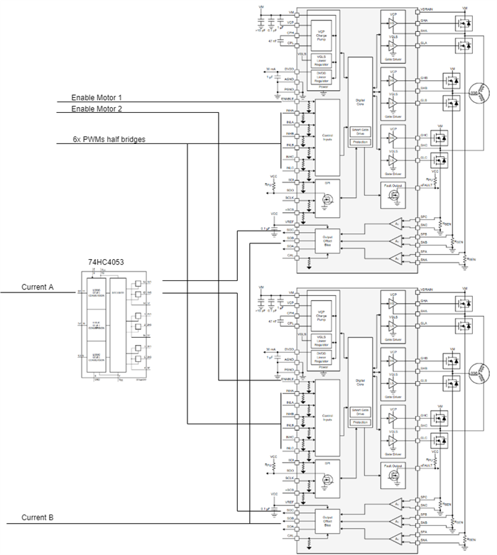
The basic idea is to use the ENABLE signal of the DRV8323S to select a gate driver. The individual half bridge control signals are shared for all gate driver ( 6x PWM connected to 4 gate drivers). SPI is used to configure the gate drivers. The hall sensor inputs will be multiplexed with an analog multiplexer (74HC4052).

Questions:

  • Are there any general pitfalls we should keep an eye on, if we want to multiplex the gate drivers with the ENABLE signal?
    (e.g. we will need to reconfigure the registers at every start of the motor via SPI because the loss of the ENABLE will reset all the registers)


  • Do we need a analog multiplexer for the current sense amplifier or are the outputs of the amplifiers on High-Z if the Enable signal is removed?
    • We could multiplex the current signals like shown for current A
    • If the amplifier outputs go in a high impedance state, we could connect all the current feedbacks together, like shown for current


Let me know if I can provide further information to understand the application.

Thank you for your help.

  • Hi Daniel,

    Thanks for your e2e post - 

    I will take a look at this soon and try to respond with an answer tomorrow (or request further info/clarification if needed)

    Thanks and Best Regards,

    Andrew

  • Hi Daniel,

    Thanks for your patience - please see response below:

    1. For ENABLE signal multiplexing, 
      1. the way you are planning to implement this sounds okay to me. 
      2. the Enable pin has an internal pulldown, so the un-used device(s) would just go to low-power sleep mode
      3. from the datasheet section 8.4.1.1 about sleep mode behavior, it is mentioned that the SPI bus is disabled during sleep, so it sounds like you might not have to reconfigure any SPI registers if you're simply 'waking up' the device by re-connecting Enable later. 
        (assuming you keep VM/Vdrain connected and powered on for each device, so that they don't go into full shutdown mode) 
    2. General pitfalls: 
      1. Some pins require an external pullup resistor like the nFAULT and SDO pins of each motor driver.
        1. the datasheet has Table 1 titled 'DRV832x External Components' 
        2. My advice is to make sure to maintain a connection to the required pullups even if you toggle any multiplexer channel-selects in the system. 
        3. and for other things, just be aware of whether there is an internal pull-up/pull-down within the DRV IC or not.
          1. The table mentioned and the functional block diagram will be a good guideline for this
    3. Current Shunt Amplifier outputs
      1. As for whether an analog MUX is needed or not for these signals, I am not 100% sure.
      2. from the datasheet section 8.4.1.1 about sleep mode behavior, it is mentioned that the CSAs are 'disabled' but I am not sure if outputs are Hi-Z or how much leakage current would pass through.  
      3. A high-precision analog MUX here would probably help, since we would want to avoid having multiple CSAs leak current onto the same shared path
    4. PWM inputs - no concerns with this so far 
    5. Hall sensor inputs
      1. just to confirm my understanding - the hall sensors of each motor will be routed to an analog MUX and then to the MCU, right?
      2. that sounds okay to me, and my only suggestion here would be to make sure to handle the MUX channel-select logic properly in the MCU code 
        (e.g. hall sensors on on motor A get selected by the MUX, while you are trying to drive motor A)

    Thanks and Best Regards,
    Andrew

  • Hi Andrew,

    Many thanks for your detailed feedback.

    1. We will test the behavior of the SPI registers in a test setup. However, reconfiguring the registers before the start of the corresponding motor won't be to much effort on the software side.
    2. We will tie together all the NFAULT lines and SDO lines, since they are open drain (including a common pull-up). We assume the NFAULT pin and the SDO pin is not pulled down in the low power mode of the DRV8323S
    3. To avoid problems we will also multiplex the current feedback, so it doesn't matter in what state the CSA are in the low power mode. Do you see any problems in using a standard analog multiplexer like the SN74LV4052A ? I think the leakage currents between the paths shouldn't be too high to cause any problems.


      To get an idea for the precision we will probably test the current MUX in a test setup and measure the overall performance.
    1. -
    2. The Hall sensors will be multiplexed again by a SN74LV4052A. Since these signals aren't too fast, we don't expect any problems on this side. The channel of the analog MUX will be selected before the start of the motor and will stay on for the entire time during the usage of the motor.

    Thanks again and best regards,

    Daniel

  • Hi Daniel,

    Thanks for the update - 

    For the discussion point about the current feedback MUX, 

    • no major problems with SN74LV4052A - just a gentle reminder to keep the component voltage ratings in mind, throughout your system. 
    • for CSA output and Hall inputs, these should be logic-level signals, so a ~5.5V-rated MUX seems sufficient for that. 
    • it will definitely be a good idea to validate the MUX performance in your test setup beforehand

    Best Regards,
    Andrew