This thread has been locked.

If you have a related question, please click the "Ask a related question" button in the top right corner. The newly created question will be automatically linked to this question.

DRV8860: ESD Mitigation Strategy?

Part Number: DRV8860

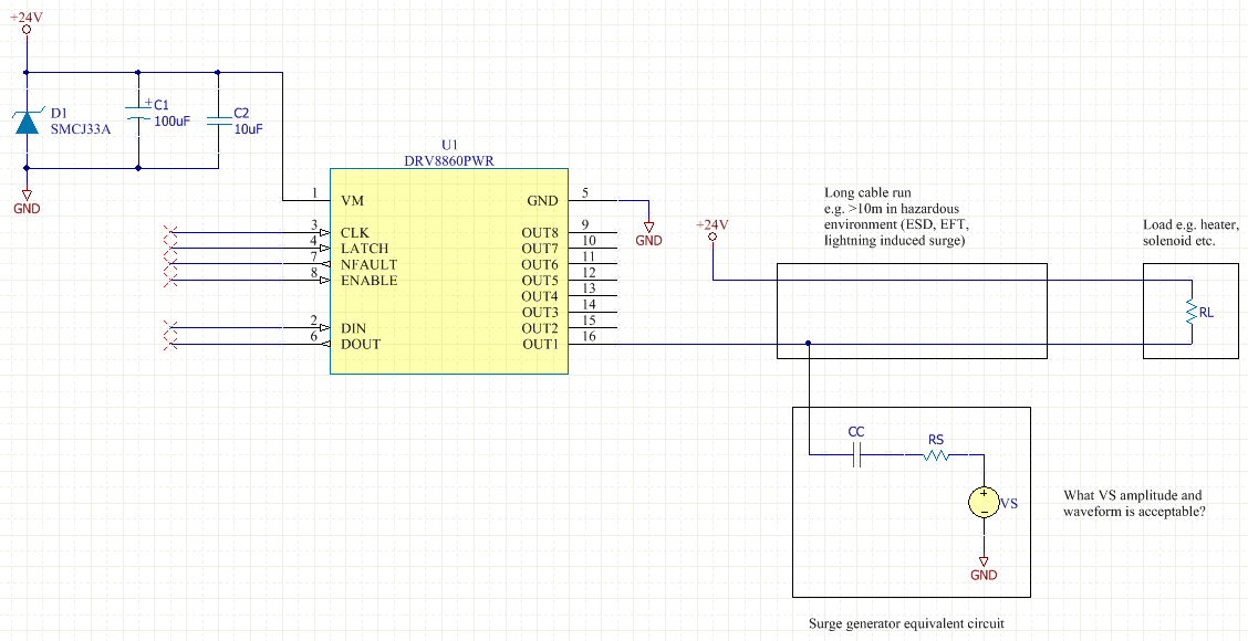
I notice this power switching device specifies only standard 2kV HBM ESD ratings on all pins.  I note also that, because it has relatively strong MOSFETs and VDD clamp diodes, it may not be so trivial to simply add e.g. TVS protection to the outputs.  What is the recommended ESD mitigation strategy for this part?  What topology or devices would be recommended or compatible (e.g. TVS, clamp diodes, peak current limiting devices)?

On second thought, would TVSs be acceptable, actually?  The absolute maximum ratings specify output voltage range up to 40V independent of VM voltage.  This directly contradicts the block diagram, which shows diodes between those connections.  Which information is correct?

Your answers are appreciated,

Tim

  • Tim,

    "On second thought, would TVSs be acceptable, actually?  The absolute maximum ratings specify output voltage range up to 40V independent of VM voltage.  "

    VM is connected to the output through the high side FET which has the body diode. It can allow the current going through from the output and VM. So, TVS on VM can also protect the output. It is acceptable to me.

    Regards,

    Wang

  • What is the continuous and peak current rating of the diode?

    Please confirm, VM and output ratings are 40V each?

  • Tim,

    VM and output rating are 40V. The diode should be able to handle 620mA OCP current. In general, the body diode only goes through the current for a short time.

    Regards,

    Wang Li

  • OK.  Would you agree that a single e.g. SMCJ33A from GND to VM, would allow the outputs to meet the full 10/1000us surge capability of the diode (Ipp = 28.2A)?

  • Tim,

    In what condition, the output has 10/1000us Ipp=28.2A surge current? 

    Regards,

    Wang Li

  • Hello,

    You said that "TVS on VM can also protect the output", what rating TVS would be appropriate?

    The 10/1000 rating is an example, with SMCJ33A being a representative part. In my particular application I am mostly concerned with ESD and EFT, which are not rated for any extra on these pins (this is unexpected, compared to other devices). I am sure others would welcome general information about transient ratings, such as for 8/20us, 10/1000us or other surge waveforms.

    Thanks,

  • Tim,

    To prevent the VM and output over voltage stress, the TVS should clamp those voltages lower than 40V maximum voltage rating. SMCJ33A looks good. 

    10/1000us spec is tested when the current goes from diode cathode to anode. DRV8860 integrated FET's body diode doesn't have any current flowing from its cathode to anode. 

    Only a forward current (from Anode to cathode) goes through the FET's body diode. From SMCJ33A spec, it is 200A which is much higher than the general working current or 10/1000us current. It has same principle. DRV8860's forward current capability could be very high for a very short period. But, in a real application, the OCP current is higher enough to charge up the input capacitor in a short time. The OCP current should not damage the body diode if the device temperature is still in a normal range.

    Regards,

    Wang Li 

  • I am not asking about OCP. I am asking about the clamp diodes in relation to an external source.

    I'm not sure how I can make this any clearer. Here is a representative schematic:


    For sake of argument, there could be incidental impedance (capacitance or resistance?) at the far end of the cable. And the cable has its own inductance and capacitance. I won't draw a complete AC equivalent circuit as it's not important. I just want to know what happens when current (of either polarity) is injected on the OUTn pin.

    Again, ESD, 8/20us surge, and other waveforms at VS would be representative. What amplitude is acceptable for each? And for which polarity, if they should differ (conduction in clamp diode vs. body diode)?

  • Hello, Tim,

    When a current is injected to OUTn pin, this current would go through the DRV8860 internal diode between VM and OUTn and push the VM voltage up until the voltage is clamped by the VTS diode. 

    The diode can allow 620mA forward current passing it. There is no cathode to anode current until the diode is damaged by over voltage spike. There is not surge test data available. 

    Regards,

    Wang Li