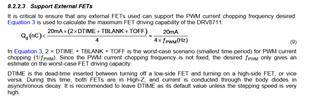
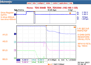
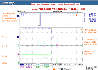
Am spinning up 10A Stepper Motor Controller using IRF4110 Fets that have a substantial Qg 150nC and total gate Capacitance of 9620pF. I have 47 Ohm gate resistors on the low side FETs.
When I step the driver via software by writing 1 to bit 2 CTRL register all works fine. If I pulse pin 10 STEP then ... .boom Both A and B side predriver fault and lockout on the first pulse. Design is currently testing at 20Vm, final design will run at 48Vm.
Also registers are as follows
ctrl = 0xE00;
torq = 0x15D;
off = 0x064;
blank = 0x032;
decay = 0x110;
stall = 0x040;
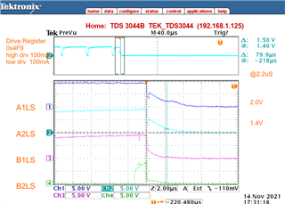
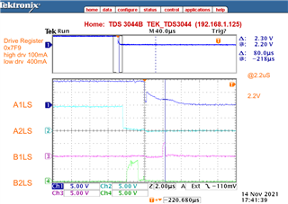
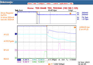
drive = 0xFF9;
I am at a loss to understand why SPI commanded steps work fine, and hardware pulse command trips PDF. Pulse input is opto isolated.
All the best,
Dave