This thread has been locked.

If you have a related question, please click the "Ask a related question" button in the top right corner. The newly created question will be automatically linked to this question.

DRV8353: High consumption

Part Number: DRV8353

Hi Team,

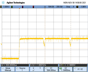
My prototype board use DRV8353RS and worked. Board is powered from laboratory supply 25V. Now consumption increased probably after reset to more than  130mA and DRV heats. VGS Status2=00000040  (VCP or VLGS undervoltage). When Enable is low consumption is OK. I tried to disconnect GHx and GLx and nothing changed. Is DRV destroyed and why? I only have one DRV left now and I'm afraid to use it until I find out the causes of the destruction.  The same situation occurred a month ago.

Thank you

Pavel

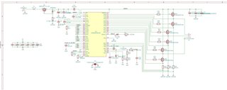
Board uses 1xPWM with HALL sensor.

Startup sequence:

During the reset is Enable held down by external resistor 10kOhm.

Program set Enable, INHx and INLx to LOW.

Than On INLA connect PWM.

Set enable to HIGH.

Set registers DRV:

Driver Control=00000040

      OCP_ACT Asociated HB is shdn.

      VCP and VGLS UVLO fault ena.

      Gate DRV fault ena

      1x PWM mode

      1PWM_COM async rect =0

      1PWM_DIR =0

      BRAKE =0

Gate Drive HS=000003FF

Gate Drive LS=000007FF

OCP Control=0000016D

CSA Control=00000283

Reserved=00000000

After this settings when DRV was still OK: set INLC HIGH motor started rotating and speed depends on PWM duty and power supply.

  • Hi Pavel,

    Can you use a DMM and measure the voltage of VCP-VM and VGLS-GND? These voltages should be ~10-12V. 

    Can you also use a DMM to measure the impedance of GHx-SHx and GLx-SLx for each phase to see if there are any shorts or opens? Comparing the impedance of these pins to another good device is a good way to check whether there is damage to the DRV. 

    Can you share your schematic and layout of your PCB as well? Usually lowering the IDRIVE setting helps - we recommend to evaluate at smaller IDRIVE settings before increasing. 

    Thanks,
    Aaron

  • Hi Aaron,

    Impedance of GHx is 1.2MOhm, GL1 and GL2 is 68kOhm, GL3 is 147kOhm.

    On scope is VGLS when DRV is enabled. Max voltage on VGLS is 3V. Now GHx and GLx are diconnected from resistors 3R3 to FETs gate.

    Thanks

    Pavel

  • Hi Pavel,

    If VGLS = 3V after multiple powerups it is likely VGLS pin is damaged. I would expect to see GLA and GLB with respect to SPA and SPB = 150kohm, so there may partial damage that results in VGLS pumping and possible ESD diode damage at the VGLS pin. I suspect there is no physical damage seen?

    May you please share schematic to investigate the components used in your system?

    Also attached are resources for help debugging:

    How to Conduct a BLDC Schematic Review and Debug

    System Design Considerations for High-Power Motor Driver Applications


    Thanks,
    Aaron 

  • Hi Aaron,

    I can not see any physical damage. DRV responds to Enable pin and communicates via SPI.

    There is schematic.

    Thank you

  • Hi Pavel,

    Thanks for sharing schematic. Only concerns I can potentially see from the schematic are:

    - ENABLE is pulled down low using 3.3k resistor, therefore it is in sleep mode and cannot wake unless external signal can drive more than 1.033mA to drive ENABLE high from the MCU. Enable is set high and the device must wake fully before running a PWM on the INHA pin, correct? 

    - VGLS cap rated for 16V, recommend 25V if current VGLS current loop is too large 


    - Ensure grounding of schematic is sufficient (split ground plane used) so that no voltage potentials exist across ground planes.

    One thing I did notice that may be causing issues is that you are using maximum IDRIVE settings (Gate Drive HS=000003FF, Gate Drive LS=000007FF), this corresponds to gate drive current of 1A source and 2A sink, which is likely causing the MOSFETs to be slammed on and off too fast and causing ringing, dV/dt coupling, or overpumping of VGLS over time due to parasitics in the layout. 

    We recommend lowering to the setting to an IDRIVE setting that results in no faster than 100ns rise or fall time of VDS slew rate, which can be calculated by Qgd / t = IDRIVE. So 1nC/100ns = 10mA IDRIVE setting, so I recommend using the mininum IDRIVE settings for your application and increase from there if faster rise/fall times are required. 

    New settings:

    Gate Drive HS=00000300

    Gate Drive LS=00000700

    Thanks,
    Aaron

  • Hi Aaron,

    INHx, INLx and Enable are connected directly to uC. uC has weak pull up resistors when reset or startup.  3.3k holds DRV disabled when uC starts. Start sequence:  set Enable, INHx and INLx low. Than run PWM on INHA. Than Enable and set registers. (it worked for more than two weeks).

    Correct sequence must be: set Enable, INHx and INLx low.Than Enable and set registers.Than run PWM on INHA. Is it correct?

    I will correct cappacitors voltage for prodution but it is not this problem. On current DPS are 50V cappacitors.

    Yes, split ground plane is used.

    I will correct max IDRIVE.

    It is possible to get somewhere at least one or two pieces DRV8353RS?

    Thank you very much

    Pavel

  • Hi Pavel,

    Thanks for sharing configuration, your sequence is correct at startup. Please let me know when you configure IDRIVE and let me know how performance changes. 

    For IC inquiries, can you please reach out to me over private messaging on E2E and I can loop you in with our marketing team. Please share your email over private messaging. 

    Thanks,
    Aaron

  • Thank you Aaron, my issue is sovled.

    Pavel