Hi I am Iri.
I had read below FAQ prior to post here. But we would like to know more detail. So let me allow to confirm again more detail.
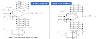
Can we use DRV8305NQPHPQ1 instead of DRV8305NPHPR without any change ?
It looks like there are slightly differential between 2 chips.
Due to supply shortage of DRV8305NPHPR now, we would like to evaluate DRV8305NQPHPQ1 very short period.
We tried to replace one DRV8305NPHPR to DRV8305NQPHPQ1.
However, replaced DRV8305NQPHPQ1 and Lch FET (due to VDS error) were broken when the motor started to be driven.
Condition:
Rch→DRV8305NPHPR (Original circuit)
Lch→DRV8305NQPHPQ1 (evaluated)
VREF: Internal VREF is not used. (External Vref is provided.)
Could you please support us and let us know whether these 2 devices are replaceable as an alternative device or not...
We are not sure that the impact of the circuit difference of DC_CAL(SPI).