This thread has been locked.

If you have a related question, please click the "Ask a related question" button in the top right corner. The newly created question will be automatically linked to this question.

DRV8328: About Power losses calculate

Part Number: DRV8328
Other Parts Discussed in Thread: DRV8300

Hi Team,

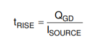
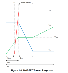
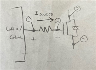
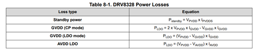
I would like to know why the formula for GVDD(CP mode)=2Vpvdd*Igvdd-Vgvdd*Igvdd.

How did this formula come about?And also how can I know how Igvdd is,I have not found this data is datasheet.

Thanks for your help.

Jenson

  • Hi Jenson,

    I am confirming the formula with systems and design teams. I believe the first part of the equation (2*PVDD*IGVDD) comes from the charge pump acting as a doubler at low voltages, since the CP acts a doubler for low voltages. But I am confirming the (VGVDD*IGVDD) part, subtracting power dissipated from GVDD rail seems confusing. 

    IGVDD should be similar to DRV8300, ranging from 400uA minimum to 1400uA maximum (800-825uA typical) in standby or active mode when no FETs are connected. If FETs are connected, average current will need to be calculated for the electrical period, which can be done by measuring the voltage across the series gate resistor. 

    I am trying to get a diagram as well to show the above equation. Please allow me some time to confirm the equation above. 

    Thanks,
    Aaron

  • Hi Jenson,

    Please look at the simplified diagram I drew below. 

    The simplified structure when operating in charge pump mode as a doubler is follows:
    1) PVDD is passed through a MOSFET and regulated if higher than the reference voltage, but since it is lower, the voltage and current gets passed through (V_PVDD and I_PVDD). 

    2) The charge pump ideally has no power loss, so assume the input power at CP = output power. Since the CP's function is to act as a doubler, then GVDD will be 2x input voltage. Since output power is doubled, input power must be doubled to maintain ideal ration, so input current will be 2x output current (I_GVDD). 

    Ideally:

    Pin = Pout
    Vin(Iin) = Vout(Iout)
    PVDD(2*IGVDD) = (2*PVDD)(IGVDD)
    PVDD(2*IGVDD) = GVDD(IGVDD)

    To calculate power loss, 
    Ploss = Pin - Pout
    Ploss = 2 * PVDD * IGVDD - GVDD * I_GVDD

    :

    Thanks,
    Aaron


  • Hi Aaron,

    Thanks for your help!

    One more question, "If FETs are connected, average current will need to be calculated for the electrical period, which can be done by measuring the voltage across the series gate resistor. "Is it related to the source current? For example, my source current is 1A at this time, and Igvdd is 1A?If this is the case, then the loss is huge. Is there something wrong with my understanding?

    Thanks

    Jenson

  • Hi Jenson, 

    I am finalizing information to calculate this, it is a descriptive process and am compiling images to illustrate process of calculating average gate drive current. 

    Thanks,
    Aaron

  • Hi Aaron,

    Thanks for your kindly help,and waiting for your feedback.

    Thanks

    Jesnon

  • Hi Jenson,

    For simplicity purposes, average gate drive current can be estimated by the following equation:


    However, you can also estimate instantaneous peak gate drive (source or sink) with the following equation:


    where t_rise is the rise/fall time of the MOSFET's VDS slew rate. 

    When VDS slews, this is during the Miller plateau of the MOSFET's Vgs waveform as shown below. 


    To calculate the Miller plateau on an oscilloscope, you'll need to measure VGS with a differential probe, or calculate the gate voltage and source voltage on separate channels then use a math channel to calculate the difference. 

    For the gate voltage waveform, you'll also probe before and after the series gate resistor to measure the voltage difference across the resistor during the Miller plateau. The voltage difference across the gate resistor during the miller plateau, divided by the resistance value, yields the instant gate current as well. 

    I've drawn where to probe below to measure the gate waveforms. 


    Thanks,
    Aaron

  • Hi Aaron,

    Thanks for your reply,

    So we calculate the loss Ploss = 2 * PVDD * IGVDD - GVDD * I_GVDD,

    According to this formula, the maximum value of I_GVDD is 1A,So the maximum loss is 24W right?

    According to your average gate current formula,I would like to know what "MosFET switching" mean?

    Thanks

    Jenson

  • Hi Jenson, 

    Aaron is currently out of office and will return Tuesday next week, so that might be a better time for him to answer on the power loss situation.

    For your second question pertaining to average gate current formula, the theory is:

    • MOSFETs take a certain amount of charge in order to turn on/off (This is Qg spec) 
    • there are many MOSFETs in the system (this is # MOSFETs Switching) 
      • Example in a 3-phase-BLDC system, there are 6x MOSFETs -> so we need to charge 6x as many Qg than if we were just turning one MOSFET on/off
    • these MOSFETs are turning on/off many times per second (this is the Switching Frequency) 
    • In total, the formula will tell you how much current on average is being drawn from the charge pump or VGLS regulator to provide source/sink current

    Please let us know if this clarifies your question about the # of MOSFETs switching 

    Best Regards, 
    Andrew