This thread has been locked.

If you have a related question, please click the "Ask a related question" button in the top right corner. The newly created question will be automatically linked to this question.

DRV8353: DC offset variations problem

Part Number: DRV8353

Hello,

We are currently designing a low-power brushless motor controller and have some issues with the currents DC offset calibration. We are using both HW and SPI versions of the DRV8353 (RS and FH) and can replicate the problem on both units.

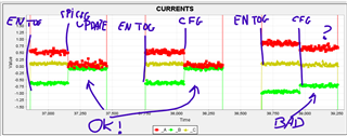
Our approach to DC offset calibration is to move the motor in an open-loop control mode to measure each phase current amplitude (find min/max values) and set each offset so that the waveforms are perfectly in the center around zero. This calibration works really well, even better than simply measuring the startup offsets to zero level and subtracting them. Here's proof for that: 

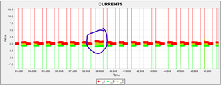
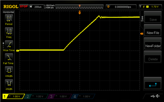
simple calibration (done during every startup, simply average measured DC offset and subtract so that the zero-current level is at true zero) 

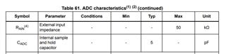
calibration during openloop movement: 

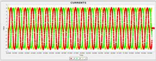
there's clearly an improvement in the waveform alignment which results in smoother operation (especially in haptic devices).

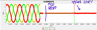
However, this is where the problems start - in order not to repeat the open-loop sequence the offsets are just saved in flash memory after the initial calibration routine. They stay the same after each power-up. This is not the case when it comes to the DRV amplifier "zero" level. It's clearly noticeable that the DRV changes its amplifier output zero levels between start-ups, that are even a few seconds apart. Actually, even an MCU reset can cause problems (essentially just toggling EN pin - the DRV is in 3x PWM mode so EN is shorted to INLx). 

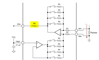
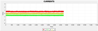
We are using only phases B and C for measurements, the A is determined from Kirchoff's current law. 

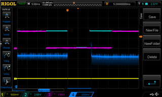
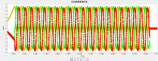
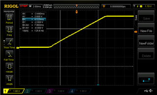
GOOD calibration outcome:

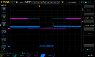
WRONG calibration outcome:

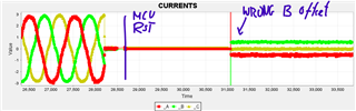
You can clearly see that before the calibration the determined offsets were correct, bringing all three waveforms to the same level. However, after the reset, the B phase is off, even though the offsets are read from flash memory.

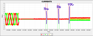
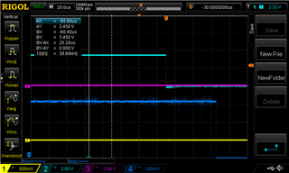
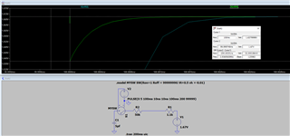
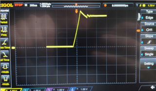
Initially, we thought it's related to the lack of the CAL pin and the automatic routine that is performed in the first 50us after the VREF crosses the minimum voltage level. The voltage level on VREF during startup is not that clean due to the buck starting up (the voltage is measured directly at the VREF cap with spring oscilloscope contact):

SPI version (with integrated buck):

Hardware version (external buck):

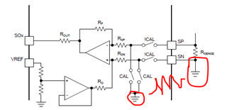
As can be seen, there are some voltage ripples near the 3.3V level, especially in the SPI version with a built-in buck. Looking at this and the internal diagram:

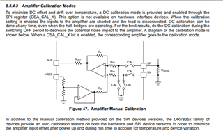
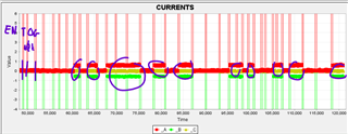
We saw that VREF is one of the sources that can disrupt the calib process since SP/SN are totally disconnected. Since autocalibration needs around 50us it seemed to be quite a good guess and this is why we made the soft start of the external buck in the HW version much longer:

This unfortunately did not solve the problem. 

It seems that it's a random problem that causes the B phase to diverge from the initial offset. It's must be an issue with DRV internal autocalibration, since it physically changes the "zero-level" voltages on its amplifier outputs (for example from 1.63V to 1.67V on the SOB pin). 

This seems to affect only the B channel, as C is always correct after the startup and calibration routine. The direction in which the B is off is random:

Do you have any ideas what could be wrong? 

Best Regards,

Piotr Wasilewski 

  • I've done some more tests and it seems a simple EN pin toggle can break the B offset:

    SPI version:

    where TOG is reset EN pin wait 300ms set EN pin, wait 300ms, perform SPi update. It's clearly visible that once in a while the B offset is off, but sometimes it gets better ofter the SPI config upload. 

    The next image is for the scale of how often the offsets fail:

    This seems to be a more often anomaly on the HW version:

  • Hi Piotr,

    Thanks for explaining the issue in great detail. This could be due to incorrect timings in the 3x PWM mode application. Just to recap, the sequence you were doing before was:

    - Open loop calibration
    - Save amplitudes in flash memory
    - Calculate A,B, and C offsets using 2x CSAs
    - Toggle ENABLE low
    - Toggle ENABLE high
    - SPI configuration
    - Run motor algo using calculated phase current offsets (issue is that CSA offset is not VREF/2 every device turn-on, seems to change)

    Since you mentioned you are using 3x PWM mode and INLx is tied to ENABLE, my first concern is that when ENABLE is taken low, the PWMs should be low beforehand to allow the gate drivers to toggle off. It takes about 400 us for the gate drivers to fully shut off after ENABLE goes low. 

    Secondly, when ENABLE is taken high, you need to wait 1 ms for the device to wake again before toggling PWMs. Since ENABLE = INLx, GLx will be on and this could be problematic in the calculation. I think the device expects the gate drivers to be in a Hi-Z state so that the CSA inputs can be shorted to GND with respect to the device GND. Rather now, having GLx on means SNx is shorted to motor ground, and SPx is shorted to device ground, so there could be some impedance difference between the two causing a difference in CSA offset every time the device is turned on. 


    Finally, the specs input offset error (Voff) and drift offset (Vdrift) may also be affecting this calculation, especially if the difference between VSP and VSN is slightly off from 0V due to the reasons above. 


    Can you please share the SPI settings used when configuring the DRV8353RS? Any main differences between DRV8353RH default settings and DRV8353RS configured settings?

    Thanks,
    Aaron

  • Dear Aaron, 

    Thank you for your analysis! In order to make sure I conducted the following experiment: 

    I cut the connection between EN and INLx. I connected INLx to a free GPIO leaving the EN connected to the previous GPIO. During toggle event I did the following steps: 

    - turn off timer outputs

    - wait 10ms 

    - INLx set low

    - wait 10ms 

    - EN low

    - wait 10ms 

    - EN high

    - wait 10ms 

    - INLx set high

    This sequence can be seen on the scope below: 

    where CH2 = EN  , CH3 = INLx, CH4 = SOB

    here's the transition form good offsets to bad offsets:

    Here's what I've found out - when the SOB is transitioning form "correct" offset to "bad" offset (and vice versa) the "bad" offset part is very noisy. After zooming in and measuring noise frequency I can see it's around 40kHz which is close to our FOC loop. The timers are off, though. This must be the ADC that is charging it's internal SAR capacitor. You can see it clearly here:

    I hope the negative spikes on ch4 are visible. 

    Is it possible that the DRV changes It's SOB pin impedance somehow? When I place a small capacitor between SOB and GND the issue is much less common (like two times in 200 EN toggles, whereas without it it's like 100 in 200 toggles)

    Best Regards,

    Piotr Wasilewski 

  • Hi Piotr, 

    If SOx outputs are noisy, we highly recommend placing an RC low pass filter on the CSA outputs to filter high frequency noise. Typically on our EVM we implement an RC low-pass filter of 56 ohm, 2200pF (cutoff frequency ~1 MHz), which reduces switching noises on SOx since these are higher frequency, sensitive outputs that can couple motor noise or switching noise on the PCB. We usually recommend a cutoff frequency that is at least 10x the PWM frequency, but you may choose the RC components as needed depending on the ADC architecture used, settling time of the CSA outputs, and load capacitance supported by the ADC. 

    Are there any low pass filters on the SOx outputs? What PWM frequency are you running your FOC loop at? 

    Thanks,
    Aaron


  • Hi Aaron,

    I understand if someone wants to filter the switching noise, but this is the ADC sampling that causes the problem, as the PWM timer is completely off, which I have double-checked (of course low pass would help here too but isn't that masking the real issue?). Is Rout really that high that the ADC can disrupt the readings? Why is it happening only occasionally and only on the B phase? Do you have any ideas?

    EDIT: sorry I missed your questions - we run FOC at 40kHz, and do not have any low-pass filters on SOx pins. 

    Thank you,

    Piotr

  • Hi Piotr,

    Something I discovered is that R6 does not actually exist in the datasheet, therefore impedance from SOx output is variable based on the GAIN setting used. I am not sure if output impedance changes with frequency as this characterization data exists, so this may explain some root cause with seeing different CSA outputs depending on the PWM frequency. Does this offset improve with higher/lower PWM frequencies?


    How much load capacitance is the internal SAR? I'm not sure how much load capacitance affects the SOx output, or even parasitic capacitance on the SOx trace. 

    If the issue still persists, is it possible to return back to the intended way of CSA calibration through the device in hardware? Typically customers implement the RC filter at the SOx output and use the CAL pin to calibrate upon device powerup before enabling the device and applying PWM outputs. 

    Thanks,
    Aaron


  • Hi Aaron, 

    Today I didn't get a chance to test the lower/higher PWM frequencies, but actually, this modification is off the table since we have optimized our system for 40kHz. 

    However, I've found these specs:

    can we assume that at DC the R6 is around 1k (based on the above specs)? 

    The STM32G4 ADC specs: 

    I have run a simple LTSpice simulation based on these specs and measured how much a 5pf cap with 50k in parallel can drain the SOx pin voltage (the green voltage is the voltage between the 50k and 1.1k resistors):

    It's around 30mV which is far from the measured 200mV spikes (when the offset is "wrong") but closer to the 80mV spikes (when the offset is correct). I'm aware I didn't add any trace parasitics or did not consider the oscilloscope probe, this is just to see what range of voltages we're talking about - they seem to be ok. What do you think about that? Can it be a DRV's internal error? 

    "If the issue still persists, is it possible to return back to the intended way of CSA calibration through the device in hardware" What do you mean by that? Like if we can use the "simpler" method for getting the offsets (not the open-loop rotation one)? I really would like to stick to the improved version since we need a smooth operation and we plan on implementing cogging compensation so the offsets must be as accurate as possible. 

    "Typically customers implement the RC filter at the SOx output and use the CAL pin to calibrate upon device powerup before enabling the device and applying PWM outputs." This however cannot be done on DRV8353 since it has no CAL pin :/ 

    Best Regards,

    Piotr Wasilewski 

  • Hi Piotr, 

    Just giving a heads up that Aaron is out of office for next few days.

    We may need some time to evaluate this information further -> and can try to aim for a response by early next week 

    Best Regards, 
    Andrew

  • Hi Piotr, 

    Thanks for your patience. VREF is not related to SOx output current, so we cannot assume 1k input impedance. I believe there is a relationship between PWM frequency, input impedance, and output impedance, but we do not have characterization data on that. I can confirm tomorrow with design whether if there exists any measurable output impedance, and how a 5pF sample capacitance from the ADC can affect these measurements. Please allow a more formalized reply tomorrow. 

    My apologies, there is not a CAL pin in DRV835x. 

    Thanks,
    Aaron

  • Hi Aaron, 

    thanks for your response. I've done some more tests on the SPI unit, and although it doesn't seem to be affected by the ADC sampling, it just randomly changes offset values. It's really hard to debug this issue as this occurs randomly on different PCBs (two with HW DRV and two with SPI). Placing a low-pass filter on the SPI version as you suggested, just adds another voltage level on which the offsets can end up after EN toggle (so there are three instead of just two different states the offsets can be), however, the problem still occurs. 

    Best Regards,

    Piotr Wasilewski

  • Hello Aaron, 

    Are there any updates on this topic? 

    Best Regards,

    Piotr Wasilewski

  • Hi Piotr,

    My apologies, this wasn't in my inbox since you may have accidentally pressed the "This resolved my issue" in your reply above. 

    I need to revisit this, I spoke with design on potential root causes but cannot find my notes from before. Can I please give a more formalized reply tomorrow?

    Thanks,
    Aaron

  • Hi Piotr,

    1) You said before VREF was not clean before. DRV835x has an automatic CAL routine at startup, so even though there's no CAL pin, it will calibrate based on the VREF voltage present at that moment once the device has waken up. Can you confirm with an external steady VREF voltage if the offset goes away or still appears?

    2) Other notes, does the supply input change when the ENABLE pin is brought low? We want to see if BEMF impacts the CSA offsets. 

    3) Does this issue happen across multiple devices/PCBs? Have you performed an ABA swap with a good device/PCB to see if it's more a device or application issue? Does this happen at certain temperature or supply voltage?

    If we still can't deduce the root cause, we can try to reproduce in lab to see if the CSA offsets differ when motor is spinning. But I think point (1) may be the best possible cause so far. 

    Thanks,
    Aaron