This thread has been locked.

If you have a related question, please click the "Ask a related question" button in the top right corner. The newly created question will be automatically linked to this question.

DRV8316: Output Duty Cycle doesn't match input

Part Number: DRV8316

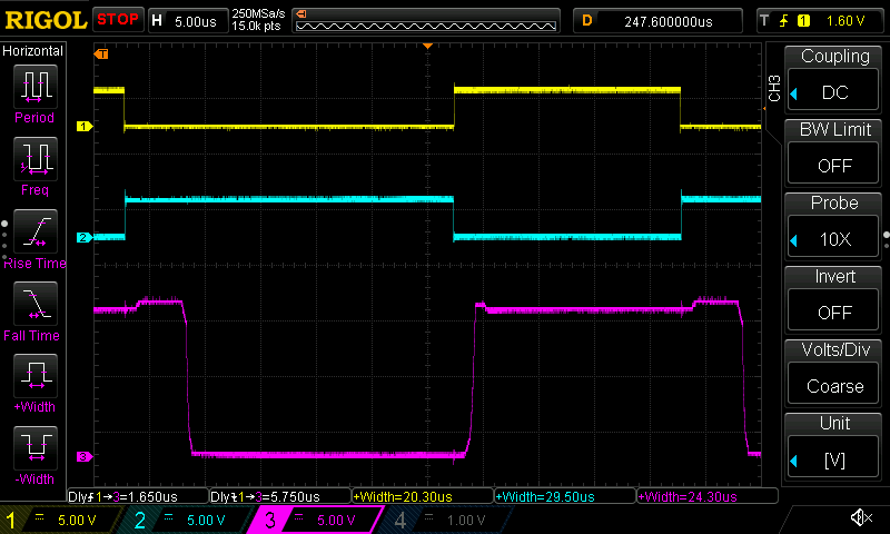
When running a calibration procedure, the DRV8316 output does not seem to match the input duty cycle.

I am using 6x PWM (not current limit mode); I have configured the device over SPI, currently with the defaults other than OCP_DEG (0x2: 1.1us), and OCP_LVL (0x1: 24A). My PWM is 20kHz, and contains 500ns of dead time between HA/LA as per the nominal dead time listed on the datasheet. (Note that AAR and ASR are off by default)

For calibration of phase resistance, I force a set amount of current (3A) through a specific motor phase using a simple PI loop for 1 second, and record the estimated phase voltage based on the requested modulation. The current is correct, measured at 2.95A; however the PWM duty cycle the PI controller applies to reach that level implies a much higher modulation than is actually seen on the motor phases.

I have tried to use the Driver Delay Compensation to make the output duty cycle match the PWM inputs more closely, and it does work to make the duty cycle less distorted. However, even using the highest delay target (0xF) of 3.2us, the output is still significantly distorted to make the calibration significantly different than expected.

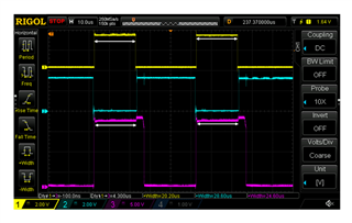
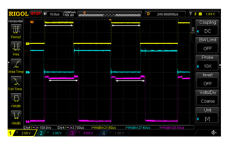
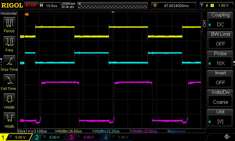
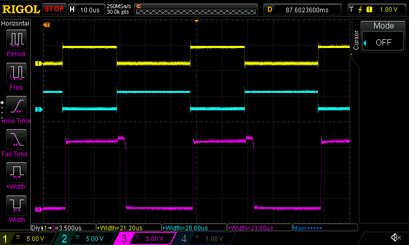
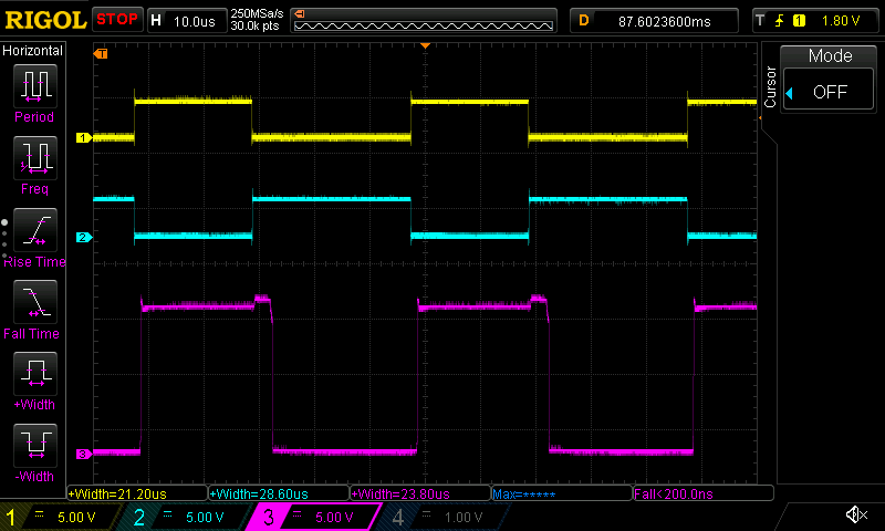
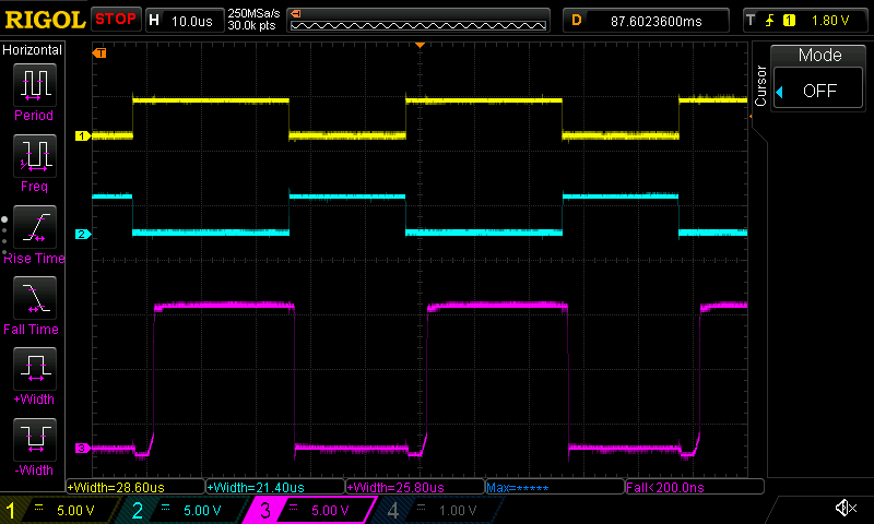
I have attached a zip of some oscilloscope traces showing the delay and duty cycle distortion. If anyone has any idea on how I might be able to make the applied duty cycle more accurately resemble the input PWM, I would appreciate it!

Thanks,

Eric

 DRV8316_PWM_distortion.zip

  • Hi Eric,

    I looked through your waveforms, I think you were okay before you configured the highest delay target value. 

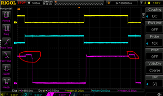
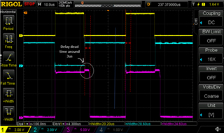
    Look at the old waveforms, your INHx inputs match the length of OUTx outputs. The arrow lengths are the same, so the INHx length and OUTx = VM length match. The purple "blips" before and after the arrow is the internal MOSFET's body diodes catching, which equal the dead time between FETs switching. This is not part of the output duty cycle. 


    Conversely, when delay compensation is enabled and maximized, this creates too much variable delay between the INHx inputs and OUTx outputs, causing a mismatch in duty cycle. The arrow lengths are the same, and you can see OUTx has shorter lengths than INHx lengths. 

    For more info on dead times and delay times in the devices, here's an app note: Delay and Dead Time in Integrated MOSFET Drivers

    Thanks,
    Aaron

  • Thank you for the explanation, that document helped me understand that blip and why it happens. 
    After reading the document over, I'm still a bit confused on the particular length of the blip when delay compensation is disabled. You mentioned the purple blips are the body diodes catching, which is the dead time (which the datasheet says is typically 500ns, but up to 750ns maximum); but on my trace on the HA to LA transition, the 'blip' is over 2.5us before it begins to decay. In the document you shared, in Figure 2-10 (which I believe is the same situation as my oscilloscope trace for the HA to LA transition) says the 'blip' should be the dead time as you mentioned, which should be constrained to the maximum of 750ns. 

    Do you know of anything that might cause this extended 'blip' / dead time? I've configured my PWM to have 500ns of dead time built in already, could that be causing anything like seen with the trace here?


  • Hi Eric,

    Looks like you may be using an output slew rate setting of 25 V/us (SLEW = 00b), which the driver will output 2500ns (2.5us) of dead time. The output dead time will be the longer of the MCU dead time or driver dead time. 


    Thanks,
    Aaron

  • I've confirmed I have been using the 200V/us slew rate (0x3 to the register)

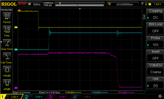
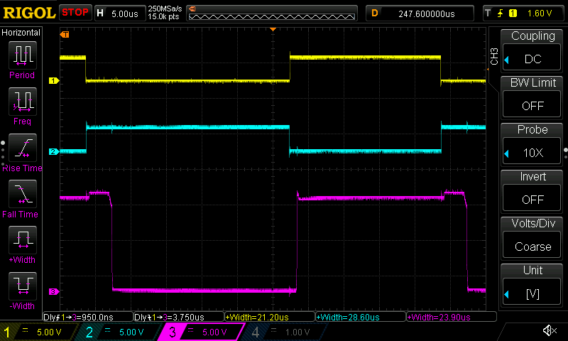
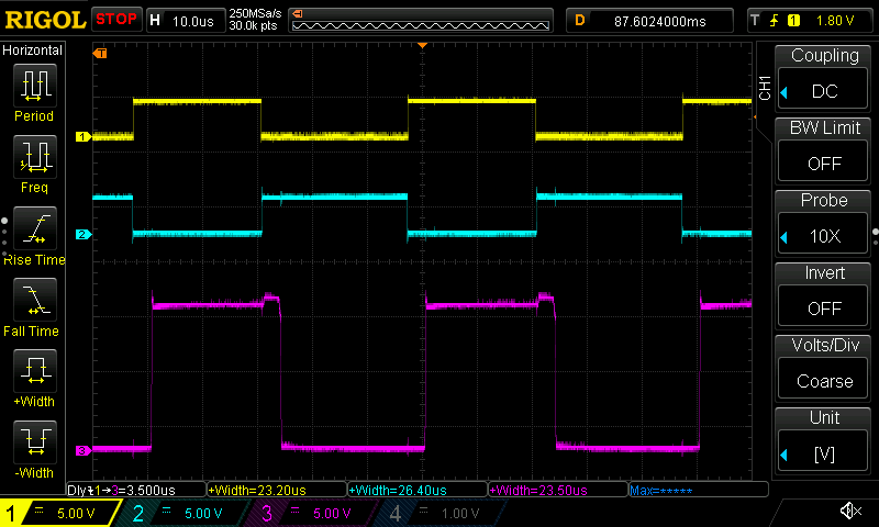
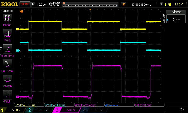
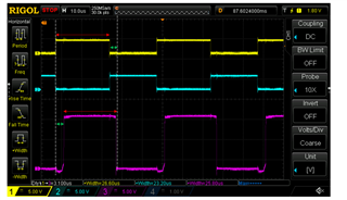
    Here's two waveforms, the first with the slew rate as I've been using it (0x3):

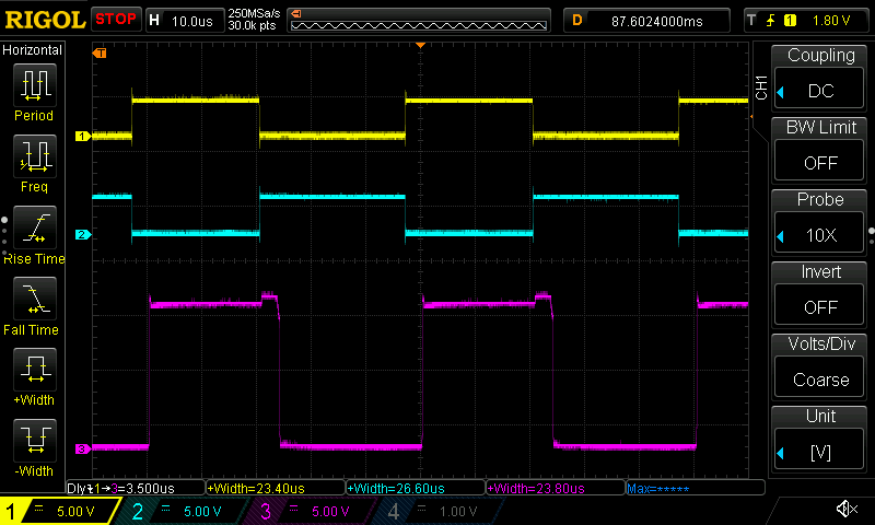
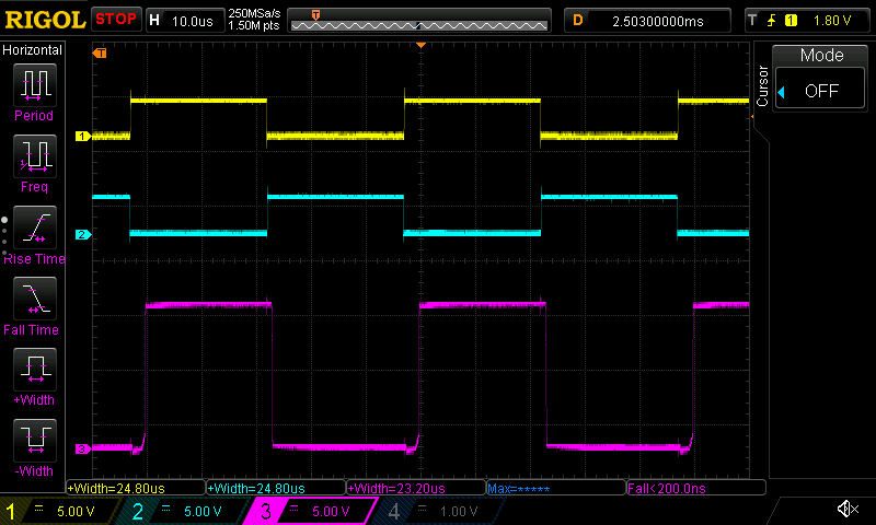
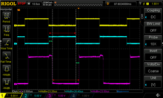
    And another waveform when I only change the slew rate to 25V/us (0x0):

    Using slew_rate = 0x3 gives a shorter dead time 'blip' by about 1-2us, but it is still well over the 0.75us maximum listed on the datasheet for that slew rate. 

    Note: for both of these, I have delay compensation enabled, and set to 1.2uS target (0x5).

    To clarify the hardware, I have the BLDC motor connected directly to the OUTx pins, with nothing else on those nets. Is that the correct implementation or could there be an issue with my hardware?

    Thanks for going through these issues with me!

  • Hi Eric,

    Enabling delay compensation to 1.2us means OUTx will follow INHA input going high by 1.2us, so a variable delay is added to match the total delay time (tpd + tdead) if dead time is less than typical in certain situations. I agree with your assessment though that these dead time periods are way longer than expected at SLEW = 200V/us. The dead time is longer than the Delay Compensation time, so it's mismatched. 


    I reached to systems to see if this is normal behavior from DRV8316, in case if layout is not optimal or internally the HS MOSFET gate is not fully off before turning on the LS MOSFET. 

    What are the specs of the application? Current and voltage? Trapezoidal or sinusoidal current? 

    Would you mind sharing schematic and layout of the application?

    Thanks,
    Aaron

  • This is the current debug configuration:

    Voltage: 12-16v

    Current: Calibration current is 3A (measured as sunk through a single phase*)

    Trapezoidal vs Sinusoidal : Sinusoidal current


    *Note: During this calibration procedure, I force a static 3A alpha (with 0A beta current: clarke transform) current, where effectively one phase sinks all the current, and the other two phases are driven the same and each supply half of the sunk current.

    Here's the schematic, plus images of the layout (It is a 4 layer board). I am happy to share other types of the board files (open source), let me know what might be useful if you need something beyond the layout images.

    BladeDrive_schematic.pdf

  • Hi Eric,

    Your schematic and layout seem fine, I don't see any probable causes of concern. I am unsure of how the 3-A alpha current (sourced via 2 phases, sinks through 3rd phase) affects the dead time, I have reached out to systems in regards to that. I'll get you a more formalized reply tomorrow. 

    Thanks,
    Aaron

  • Hi Eric,

    Can you check a couple of things for me:

    Can you rerun the test using <500ns or 0ns dead time from the MCU. If current is flowing into the phase (high side diode conducting), it will try to maintain its "off" time and not its "on" time.

    Can you also measure Phase A and Phase B while running the test? Are those dead times affected?

    Thanks,
    Aaron

  • In my most recent oscilloscope trace I shared showing the difference between slew 0x0 and 0x3, the MCU had the dead time set to ~100ns. 

    This evening I can measure phase A and B, do you mean the OUTx nets (I have a 4 channel scope, so I can't measure the HA/LA while measuring all outputs)?

  • Hmmm okay, thanks for letting me know.

    Can you measure INHA/INLA/OUTA (like above) during the calibration phase, and then measure INHB/INLB/OUTB and INHC/INLC/OUTC as well? These can be separate scope shots, but ideally it should be during the calibration phase. We want to see if dead time performance is correct when current goes into the phase (i.e. OUTB, OUTC) versus out of the phase (OUTA).

    If you'd like, change the MCU dead time to 0ns as well to see if dead time is more consistent. 

    Thanks,
    Aaron

  • Here are those three traces; I extended the calibration time to 10 seconds to ensure the PI loop had converged on a set value (normally only 2 seconds is sufficient). So the traces should be taken when all PWM times are about the same during each separate capture.

    I left the same dead time as my last reply, and is measured right at 96ns as it's set to. The slew rate was set to 200V/us (0x3) for all these captures.

    **EDIT: This is with a delay target of 3.2us (0xf)** 


    OUTA and OUTB are identical, as I'd expect, and OUTC has about the same length 'blip' as A and B. 

    I measured the OUTC 'blip' at 2.46us before it starts slowly increasing until it shoots up.

    OUTA:

    OUTB:

    OUTC:

  • I captured all the 6x pwm signals with my DSA, if you want to see all the PWM inputs at once. I attached the data as a Saleae file (https://www.saleae.com/downloads/), but can convert it to something else if you can't open that.

    (Note this is the exact same firmware/hardware as the last post with OUTA/OUTB/OUTC traces, so the PWM should roughly match up)

    DRV8316_Calibration_INx.sal

  • Hi Eric,

    My Logic software is outdated and it's not opening it up. Can you share in another format please?

    Thanks,
    Aaron

  • Here's a CSV of the end of the Saleae capture (the full thing was over 50MB as a csv), as well as a screenshot of a couple cycles that's easier to visualize.

    partial_DRV8316_Calibration_INx.csv

  • Hi Eric,

    Thanks for sharing. I misread an earlier reply, you are sourcing about 1.5A through two phases and sinking the total current of 3A through the third phase. Were you able to see OUTx have similar dead time blip periods on all three phases? Were any other phases correct (1.2us) when DLY_TARGET = 1.2us?

    Can you also try at a smaller calibration current, say 500mA + 500mA source and 1A sink, to see if the OUTx dead time blips improve?

    Thanks,
    Aaron

  • Here are the same traces, with delay target of 1.2uS, but they look nearly identical to the previous waveforms with the 3.2uS target: 

    (The previous ones were 3.2uS, I've edited the post to clarify that)

    I also tried to scope OUT_C after changing the calibration current to sink 1A through C, and there isn't much difference than less ringing/overshoot on the OUT_C pin. The 'blip' is about the same length as the 3A trace, at just a bit over 2uS before it starts slowly rising. But none of them are near the 1.2uS target 
     

  • Hi Eric,

    Thanks for sharing. I will get a more formalized reply next week after looking more in depth. 

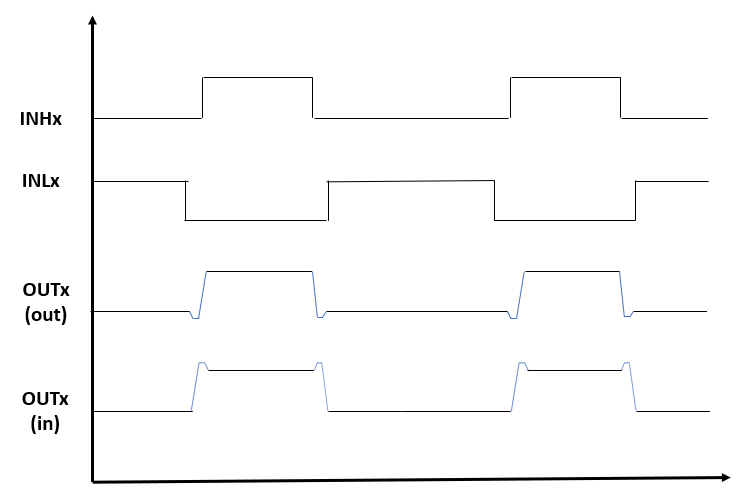
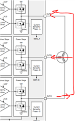
    Are you sure the waveforms above are matching your expectations for OUTA, OUTB, and OUTC? If current goes out of the phase, the OUTx body diode blips will be around -0.7V. If current goes into the phase, the OUTx body diode blips will be around VM+0.7V. See below. 

    Have you tried this test before on a DRV8316REVM, if so, have you seen a similar issue? Have you tried just applying INHx/INLx as synchronous waveforms without a motor to see if dead time is normal? Not sure if the motor is somehow affecting the deadtime. 

    THanks,
    Aaron

  • (Delay Compensation set to 1.2us)

    I do not have an EVM, so I'm not sure If I'd see it on that. Here's some traces of OUTA (current intended to flow out of OUTA), without any motor attached.

    Without a motor, there are (much smaller) diode blips when the OUTA pin goes high, and no blip giving a more expected propagation delay/dead time when the OUTA pin goes low: 

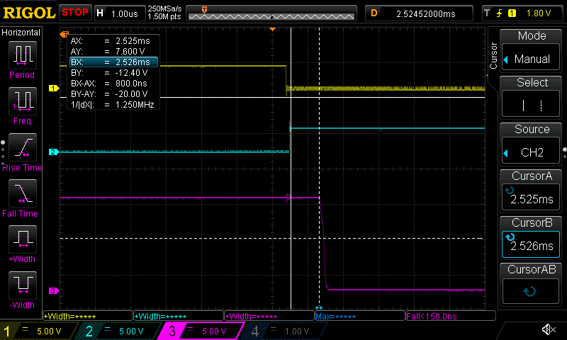
    I'm measuring about 800ns between INLA going high and the OUTA pin going low:

    With INHA going high, and OUTA going high, there is about a 2.6us delay:

  • Hi Eric, 

    I was incorrectly looking at how Delay Compensation occurs in your waveforms above. I was looking at the dead time rather than the delay inserted by the DRV8316 to match INHx --> OUTx "on" times and INLx --> OUTx "off" to reduce duty cycle distortion. It is actually working correctly from your waveforms above and I'll re-explain using your images. 

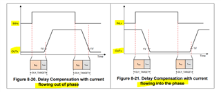
    Duty cycle distortion occurs from incorrect timing due to propagation delay and current measurements, which depends on current direction of OUTx pins. In the two cases below, the OUTx "on" or "off" time may be shorter than the input on/off time due to delays in the DRV8316. Therefore the variable delay time for the total DLY_TARGET time is added in the two cases below:

    1) INHx "on" time matching OUTx "on" time when current flows out of the phase
    2) INLx "on" time matching OUTx "off" time when current flows into the phase 

    So we need to investigate the time between the input rising and the OUTx rise/fall depending on the current direction (not the dead time). This is where I made the mistake above. What you're measuring above is the inserted variable delay time (tvar) after the dead time to ensure the duty cycle ON/OFF times match correctly, so depending on the current direction, the "blips" are longer than the spec'd dead times for the slew rate setting. 

    Let's look at your OUTA/OUTB/OUTC waveforms. 

    OUTA:

    OUTB:

    OUTC:


    First of all, because of how the body diodes catch (dead time blips that appear), current is sourcing out of phase C and sinking into phases A and B. 

    Let's start with OUTC, which is sourcing current. To ensure the OUTx "on" time matches the INHx "on" time (red), delay compensation can be added (green) to allow OUTx to delay the OUTx output slewing. By doing this, the device has more time for the sink currents to calculate current, switch appropriately, and overcome mismatch in propagation delays. When set to 3.2us, we see the driver adds variable delay time to remove duty cycle distortion. 

    Now let's go to OUTA, which is sinking current. To ensure the OUTx "off" time matches the INLx "on" time (red), delay compensation can be added (green) to allow OUTx to delay the OUTx output slewing. By doing this, the device has more time for the sink currents to calculate current, switch appropriately, and overcome mismatch in propagation delays. When set to 3.2us, we see the driver adds variable delay time to remove duty cycle distortion. 

    Hope this helps!
    Aaron

  • Hi Aaron,

    That does help my understanding of the feature greatly!

    I see the feature is working perfectly as expected in the images you marked up (which had the delay compensation set to 3.2uS). 
    Looking at the images (with a motor), when I have the delay compensation set to 1.2uS (as recommended for my slew rate), the waveforms don't quite match what I'd expect after reading your comments. Specifically, the first two waveforms are sinking current, so by my understanding the OUTx 'low' time should match the INLx high time? For some reason, the first waveform (OUTA) is low for about 27us, while INLx for that cycle is high for 28.6us; and OUTB is about identical.

    Then OUTC which is sourcing current should have the OUTx 'high' time matching the INHx high time; but again OUTC doesn't seem to match that.

    Based on that, does it seem appropriate that for some reason my system needs the delay compensation set to 3.2uS to get as accurate a duty cycle as possible?

  • Hi Eric,

    Going back to your original waveforms from your zip file, I agree that a delay compensation default value of 1.2us is not enough for your motor because the OUTx dead time at the first interval between INLX going high and OUTx going low is long, around 3us. This can be due to higher inductance motors and driver delay times to switch the motor current. Even though the second interval is very short and near 1.2us as programmed, you need to use a delay compensation time that is at least the value of the longest delay time during an input transition - in this case, around 3us. 


    With the lower settings, there is still mismatch between INx and OUTx, which is what you were seeing before between 27us and 28.6us. So therefore around 1.6us more of delay compensation should be added (on top of 1.2us) to reduce the difference between INx and OUTx. Therefore the delay compensation should be set to the max (3.2us) to get as accurate a duty cycle as possible.

    Thanks,
    Aaron

  • Hi Eric, 

    To resolve this issue, please ensure Bit 6 in Control Register 3 is set to "1", this removes the long dead time issue. In the pre-RTM datasheet, this was set to a "0" by default and causes long dead times. The RTM datasheet will have this bit corrected to a "1" for default. 

    Thanks,
    Aaron