This thread has been locked.

If you have a related question, please click the "Ask a related question" button in the top right corner. The newly created question will be automatically linked to this question.

DRV8350F: Gate Driver dies quickly (permanent GDUV fault)

Part Number: DRV8350F
Other Parts Discussed in Thread: DRV8350, DRV8306EVM, DRV8332, DRV8312

Dear Team,

we are having an issue with our motor controller design and have run out of ideas on how to resolve it. The gate driver dies very quickly.

We are using a DRV8350FS to control the half-bridges (Vishay SIZ260DT) of a BLDC motor (maxon 70W EC45 402685), the schematics are attached in the google drive link below.

After booting our microcontroller (STM32F373), we configure the DRV8350FSRTVR as shown on page 3 of the schematics. We use a PWM frequency of 32kHz. The configuration seems to work somewhat as the motor successfully starts to rotate. However, after a while (few minutes), the motor controller signals a VCP / VGLS undervoltage lockout fault and gets very hot (far beyond 100 °C for an ambient temperature of 20 °C).

After reaching this point, the fault is signaled constantly, even after rebooting the board (i.e. toggling power supply) and even if the board was unplugged for hours. We also removed the half-bridges to check if the error persists with no load, which it does.

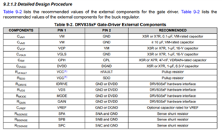
For broken boards, the voltages at VCP / VGLS pins are less than 4V above their reference potentials of VCC / GND. For good boards, voltages are roughly 15V above their reference potentials.

We are constrained by space and thus left out the bypass capacitors of the half bridges, but have followed the other design recommendations as far as we can tell. Can these be the reason that the drivers die so quickly or did we make other mistakes?

The gerber files are attached as well, in case our layout is causing problems.

Any help is greatly appreciated and we will happily provide any further information you require.

Best regards

Mike & Lukas

Attachements:

drive.google.com/.../1OhSuu6E4-viXDdQTjSsko-YGo6D1j251

  • Hi Mike, Lukas,

    Thanks for reaching out via our e2e forum!

    I will look through the schematic and layout files within the next few days to screen for issues and will give feedback on anything that stands out as problematic. 

    For the 'broken' boards, the observed voltage differentials being <4V are definitely indicative of the GDUV fault conditions (undervoltage of either VGLS regulator or VCP regulator). The ~10-15V gate-drive voltage differential on VCP-Vdrain and VGLS-SLx in a 'good' board matches our expectation of a working gate driver system.

    One thing I am curious about is the aspect of observed damage in the system.

    • From the information provided, I am not sure if the DRV device itself is damaged or the external system-level components have been damaged, causing the DRV device to not be able to operate properly. 
    • Would it be possible at all to do a sort of A-B-A swap experiment? 
      • swap 'broken' system DRV IC onto a 'good' system PCB
      • swap 'good' system DRV IC onto a 'broken' system PCB
      • and then observe whether the damage follows the DRV IC, or the system PCB, or if both have sustained damage

    If thermals are a consideration in the system, that does sort of suggest that maybe layout or operating conditions would be root cause.

    Best Regards,
    Andrew 

  • Hi Michael,

    Just a quick review of pcb layout.

    There are no ground planes except some under MCU, what can result in:

    - overheating DRV8350 and half-bridges

    - excessive noise transfer between traces

    - more difficult power rails decoupling

    - excessive voltage drops between different parts of pcb

    - increased emi noise

    No any decoupling caps near half-bridges gives probably increased switching noise, transients and ringing.

    Traces between DRV8350 and half-bridges look quite thin and change layers twice what gives increased inductance and possible

    problems with ringing and resonances.

    70W is not a lot and I think design with solid (non-splitted) ground should work. I would try to use inner layers as ground planes as much as possible, keep all power and signal traces on top and bottom, keep high power area separated from low signal area, stich with vias any GND traces on bottom and top to inner ground planes, stich also inner ground layers together, keep traces between DRV8350 and half-bridges possibly on one layer,  quite thick and possibly short, use GND vias close to areas where those traces change layers, decouple each half-bridge with MLCC around 100nF.

    Below mentioned Application note is a good start point

    https://www.ti.com/lit/an/slva959b/slva959b.pdf?ts=1644947491124&ref_url=https%253A%252F%252Fe2e.ti.com%252F

    EVM boards could help as well like DRV8306EVM that uses TI half-bridges.

    You can try to change IDRIVE to 50mA, dead time to 400ns and check if it extends board live, I would also monitor DRV8350 and half-bridges temperatures.

    Regards,

    Grzegorz

  • Hi Grzegorz, Mike and Lukas, 

    Agreed with the inputs and resources above from Grzegorz.

    The layout does seem like the source of the problem here, especially if you are seeing problems with excessive temperature. 

    Similar to the above comments, our layout guidelines typically suggest: 

    • keeping DRV IC caps (VCP, CPH/L, VGLS, DVDD, VM, etc..) and gate-drive signals (between DRV IC and MOSFETs) on same layer without any vias in the signal path. 
    • placing these caps very close to their intended signal network (e.g. VCP cap very close to VCP pin) 
    • having thick gate-drive signal traces (15-20 mils) 
    • wide copper pours for any signal paths involving high power/current, such as MOSFET VDRAIN and system GND 

    Best Regards, 
    Andrew 

  • Hi Andrew and Grzegorz,

    thank you very much for your feedback so far, we will incorporate your suggestions into the next revision.
    However, to clarify, only the broken boards get excessively hot, and the half-bridges stay at a low temperature.
    Furthermore, we tried testing only enabling the DRV8350 without configuration and without PWM, and it still got hot even when the half-bridges were not soldered on.
    So we do think that it is indeed the chip that is broken.
    Sadly, we can’t easily swap the chips as we only have two remaining (more are on the way, but the chip shortage poses some problems).

    We will definitely use your advice, but we are worried if that alone does not resolve the issue we will have hardly any time for a second revision.
    So if you have any additional suggestions that we could try in parallel, we would like to do those too.

    Thanks and best regards
    Mike & Lukas

  • Hi Mike and Lukas,

    Unfortunately there is no guarantee that next pcb design will work even after someone else reviews it. Something that has worked for someone does not have to work for you, some issues can be missed etc.

    Using U302 decoupling cap for MCU power supply decoupling might not be a good idea unless for analog circuits.

    If I needed more space I would consider using 0402 caps instead of 0603 where it is possible (decoupling caps for 3.3V)

    Can you tell what is thickness of pcb copper layers, voltage and max. current that you expect?

    Regards,

    Grzegorz

  • Hi Mike and Lukas, 

    One other thing I wanted to ask: what is your system's nominal operating voltage for VM and Vdrain? 

    One important consideration we stress to our customers for DRV devices is to have properly rated components, especially for bypass/bulk capacitors near the DRV device inputs and MOSFET power stage. 

    The best-practices we recommend are to make sure your device has all of the necessary external components at proper values listed on the 'Figure 8-2. Block diagram for DRV8350FS' and to also reference the 'External Components' table below. 

    Especially for the CPH/L cap, VM caps, VDRAIN caps, they should be rated for 2x the operating voltage expected. 

    • This is because MOSFET VDRAIN voltage can overshoot to 2x during special operating conditions like braking

    Best Regards, 
    Andrew 

  • Hi Mike, Lukas, 

    One last thing - please see these EVM design files as the reference for your layout. 

    There will definitely be some useful reference layout to show how the grounding planes and high-power planes need to be set up

    https://www.ti.com/tool/DRV8350S-EVM#design-files

    Some resources: 

    Best Regards, 
    Andrew 

  • Hi Mike and Lukas,

    In case of pcb that you already have made I would try to place MLCC around 100nF-470nF at each half-bridge, between VCC and MGND. Probably you would have to use leaded version, please make leads as short as possible. There is some chance that it would help.

    Coming back to review. Bottom connector looks OK, power is on the left side, digital signals on the right, though NRST line is not ESD protected.

    Top connector. If possible I would place motor output lines on the left side, then GND and 5V, then all digital lines on the right. I would move all three half-bridges to the left side of pcb as much as possible, it would give enough space to route digital signals on the right side. If you went for solid ground in inner layers it would spread heat from half-bridges.

    Routing gate signals in differential pairs together with their current return lines seems to be a very good solution (except that they look thin what I mentioned before).

    Grounding ESD protection diodes like Z103,Z104 and Z105 with long trace, even thick one may not be very effective, again solid ground would be much better.

    Regards,

    Grzegorz

  • Hi Andrew and Grzegorz,

    thank you very much for your additional feedback.

    To answer your questions about operating conditions of the pcb, input voltage may range from 28.8V to 33.6V (8 LiPo cells) and load current should be less than 2.5A. The layers have a thickness of 35u each, as thicker layers cannot be manufacturer with the given trace width beneath the microcontroller.

    Hence, capacitor ratings for bulk capacitance are chosen to be 1.5 times bigger than operating voltage. During component selection, bigger voltage ratings were not possible as availability was either poor or components would have been to high (C301 and C302). For shared capacitor of U302, during layout process, its capacitor nearly overlapped with MCU decoupling capacitors, hence we removed it.

    Anyways, we will definitely try to incorporate as much of your feedback as possible and keep you updated, as soon as we have a grip on the new revision!

    Best regards,
    Mike & Lukas


  • Hi Mike and Lukas,

    Thanks for your answer. 4 layer 35um board is more than enough for 2.5A driver. 2.5A at 33V is not a very demanding design, if you have more boards I would definitely try these half-bridge caps that I mentioned earlier. If it worked it would allow you to evaluate design better before making a new revision of pcb. For 2.5A 35V driver you may be able to use some integrated solution like DRV8332/DRV8312 but DRV8350 design can be easily scaled up in future.

    Regards,

    Grzegorz

  • Hi Michael, 

    Closing the thread for now, but feel free to update us & re-open thread for support once the new revision PCB testing starts

    Best Regards, 
    Andrew