This thread has been locked.

If you have a related question, please click the "Ask a related question" button in the top right corner. The newly created question will be automatically linked to this question.

DRV8300: Design Verification

Part Number: DRV8300

Dear Team,

I have designed a gate driver for the BLDC motor drive application. Since I'm new to design I'm doubtful about proceeding with this design.

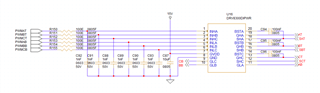
I have attached the schematic. Please verify and let me know the suggestions. 

  • Hi Adarsh,

    Thanks for your post! I looked over the portion of the schematic that you provided and have the following comments:

    1. For phase B and phase C, the bootstrap capacitors are accidentally connected to the GHB and GHC pins. These should be connected to the SHB and SHC pins just like you did for phase A. 

    2. I would strongly recommend putting gate resistors on the high side and low side gates as shown in Figure 9-1 of the datasheet so that you can slow down the gate drive current of the device if necessary depending on the Qgd of the MOSFETs you are using. If the gate drive current is too high for the MOSFETs that you are using, this can cause ringing on the gate and source of the MOSFETs during switching, and can even lead to device damage if the voltage ratings of the device pins are exceeded. Adding gate resistors will allow you to tune the gate current strength by changing the resistor value and adjusting the MOSFET switching slew rate. The Qgd of the MOSFET is a primary factor in how much gate drive current is necessary to switch the MOSFET at a particular slew rate. Lower Qgd MOSFETs will need less gate drive current to switch the MOSFET on or off in a particular amount of time compared to higer Qgd MOSFETs. 

    3. When calculating the correct bootstrap capacitor value to use, it is necessary to take into account the total MOSFET gate charge for the MOSFETs that you are using and the PWM frequency as described in section 9.2.2 of the datasheet. I don't see any issue with the bootstrap capacitor value that you chose as long as this is consistent with the calculations that are laid out in section 9.2.2.

    4. Make sure that the voltage ratings of the capacitors that you use are rated for approximately 2 times the expected voltage on the pin. This will help mitigate the effects of capacitor derating (especially for ceramic capacitors) that can occur when the voltage applied on a capacitor is close to the rated voltage. 

    5. TI has a resource on PCB layout best practices for motor drivers that may be helpful for you to read over as you start on the motor driver PCB layout. I have attached that document here.

    Regards,

    Anthony Lodi

     1602.Best Practices for Board Layout of Motor Drivers.pdf

  • Hello Anthony Lodi,

    Thank you for your valuable feedback 

  • Your welcome!

    Regards,

    Anthony