This thread has been locked.

If you have a related question, please click the "Ask a related question" button in the top right corner. The newly created question will be automatically linked to this question.

DRV8350: what it means that the GLX is shorted to vgls

Part Number: DRV8350


I see the datasheet that

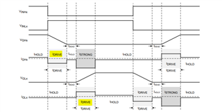
Then glx is short to pgnd and shx or vm.It means that the Idrive is too low and should be shorted to the pgnd、shx、vgl

But this days I have two pcb whose Idrive_LS and Idrive_HS are the smallst value (50mA or 100mA).But  I found that the glc pins is 

shorted to the vgls 。Does it also means that  the idrive is too low? Besides the tdrive is the max value and the ghx ara all goond.

thanks

shengzhong

  • Hi Shengzhong,

    If GLx is shorted to VGLS, then damage likely occurred at GLx in the internal pre-driver FET. 

    Please ensure your IDRIVE value is selected carefully to ensure you are not overstressing the MOSFETs or switching motor current too quickly: https://e2e.ti.com/support/motor-drivers-group/motor-drivers/f/motor-drivers-forum/796378/faq-selecting-the-best-idrive-setting-and-why-this-is-essential

    Please ensure there is no negative ground bouncing at SLx or negative gate voltages at GLx, or else you can blow up the internal body diode of the HS or LS predriver FET internally and cause GLx damage. Ensure good layout removes parasitics from the gate driver and motor current paths. You can use gate-to-GND diode to remove negative transients, or add capacitance from VDRAIN-SLx to suppress negative transients at low-side source. 

    Follow this app note more ways to reduce pin damage for higher power designs: www.ti.com/.../slvaf66

    Thanks,
    Aaron

  • hello , Aaron:

    I am shengzhong's colleague .

    Let me show you some details about our issue .

    Our Idrive was set to 100ma , so i don't think it is because of the idrive too large . If Idrive too less will cause this ?

    The current throught the mos was 0 to 10A very fast , should this be the real reason for this ?

     the attach file is our  schematic .Can you help have a look about it ?DRV8350.pdf

  • Hello Lining,

    If excessive capacitance is present at the gate drive outputs, then too little IDRIVE current can also cause potential issues as well. First, you want to ensure enough gate drive current turns the MOSFETs on and off to avoid shoot through current conditions. Ideal timing diagram is below. 

    Too slow of a gate drive current may cause VGS rise/fall time to be too long with potential shoot through if VGS > Vth for high side and low side MOSFETs. This is due to RC time constant of gate rise and fall times. The higher RC value can be caused by:

    • Gate resistors limiting gate current
    • Capacitors from gate to source
    • Small IDRIVE currents
    • Higher MOSFET Qgd values

    In reviewing the schematic, I see there are gate to source capacitors on the LS FETs. Can you remove these and see if gate driver performance improves?

    The device has selectable IDRIVE source and sink current settings, which removes the need for external sink diodes. The gate resistors are okay, but we recommend starting with 0-ohm resistors so gate current can be selected via the IDRIVE registers in SPI. 

    The MOSFETs used are 3nC Qgd, which is a very small value. We recommend the VDS rise/fall time to be no faster than 100ns, so we recommend choosing an IDRIVE setting no more than 3nC/100ns = 30mA. You do not need much gate drive current to turn on these FETs, 100mA may be slewing VDS too fast and causing damage at the GLx gates via negative transients. 

    Choose an IDRIVE setting based on this: https://e2e.ti.com/support/motor-drivers-group/motor-drivers/f/motor-drivers-forum/796378/faq-selecting-the-best-idrive-setting-and-why-this-is-essential

    Hope this helps,
    Aaron

  • Hello , Aaron:

    Thanks for your reply .

     you mentioned "Too slow of a gate drive current may cause VGS rise/fall time to be too long with potential shoot through if VGS > Vth for high side and low side MOSFETs."  the one you said shoot through is refering "DRV " or the external  mos ? If you refered to the DRV will shoot through , i don't understand about this . I think too slow "open external mos " will lead mos broken not DRV . Can you try to explain this ?

    And about the source capacitors ,we have removed it , but no help .

    And our external mos Qgd is 3nc , i will try to add res to limit the rise/fall time to "no faster than 100ns ".

    If we limit the time to 100ns , but still no help , we will try to  add the gate-to-GND diode .

    If extern mos current raise / fall quickly will lead to this damage ?  I am not fully understand about this .

    look forward to your reply .

    Thanks 

    lining

  • Hi Lining,

    I am referring to the external MOSFETs. Device uses an internal state machine to ensure GHx and GLx are not turned on at the same time via dead time. 

    Please monitor GHx/SHx/GLx waveforms and ensure that VDS slew rate of HS MOSFET (VDRAIN-SHx) and LS MOSFET (SHx-GND) is 100ns or slower to reduce inductive spiking at the powerstage. Spiking too quickly can cause damage as shown in dV/dt coupling below. 


    Please read this app note on power stage design for higher power motors: www.ti.com/.../slvaf66

    Thanks,
    Aaron

  • Is this gate-to-gnd diode the same as the one added in the high side like the picture.And is the reason why the high side GHx are working well?

  • Hi Shengzong,

    Yes, high side only includes VGS gate-to-ground diode. This is a 15-V rated Zener clamp diode to protect GHx from rising to 15V over SHx. VCP needs to be more protected than the low side VGS because VCP-VM ESD diode can be damaged if VCP increases to 15-V over SHx (or VGSH = 15V). 

    VGSL (low side VGS) can tolerate higher gate voltage because VGLS regulator is operational to 20-V max. Hence gate-to-GND diode is not in device design. You can implement an external gate-to-GND diode on the low side VGS to protect against negative GLx voltages, or mitigate inductances in the power stage. 

    Thanks,
    Aaron

  • hello Aaron:

             We seems find the problem.We check the wave of VDS.The fall time is 25ns and the rise time is also 25ns。But we have set the idrve to 

    the smallest value 100 mA. The theoretical calculation of falltime is 300 ns.I have replace the Rg  to 0Ω。Do you know why the acture fall time 

    inconsistent with the theoretical value.(100mA Rg=0   Falltime is 25ns)

    thanks

    shengzhong

  • Hi Shengzhong,

    Your Qgd of your MOSFETs are very small (3nC). 3nC / 100mA = 30ns VDS rise/fall time. Please set to min setting  (15mA source / 30mA sink). It should lengthen your VDS rise/fall time. 

    Thanks,
    Aaron

  • hello, Aaron :
    We measured the waveform between GLx and SLx.
    It was found that sometimes there is a negative voltage of 2.1V. Will this negative voltage cause DRV damage?
    At the same time we also measured the waveform between VGLS and GLx, the highest peak can reach 17V.

    Thanks

    lining

  • Hello,

    If GLx-SLx = -2.1V for a transient amount of time, it may cause damage over time based on these abs max specs. There is generally an inverse relationship (1/t) on the length of the transient time and negative voltage tolerance the GLx pin can handle between these two specs. 

    The device should be okay if it hasn't damaged yet so far over continuous motor operation, but it is best to try and mitigate these transients as best as possible during evaluation to reduce potential damage to the DRV or MOSFETs. You can use a GLx-GND diode to mitigate these transients or reduce inductance in the gate drive path by using a thicker trace (such as a wire). 

    Thanks,
    Aaron

  • Thank you very much , I found the "Absolute Maximum Ratings" in datasheet  , I will measure the waveforms at those pins .

  • Hi Lining,

    Sure thing, let me know if any more help is needed. 

    Thanks,
    Aaron

  • Hello  Aaron:

             I have a question that weather the lead process will bring more parasitic inductance near the mosfet.Since that I see the this

    the leaded mosfets

    thanks

    shengzhong


  • Hi Shengzong,

    Leaded components such as MOSFETs add parasitic inductance to the gate drive path and motor paths. Adding parasitic inductance at the gate drive path means it will take more time to change the current path (source vs sink current), so a smaller IDRIVE value, gate series resistor, or gate-to-source capacitance (Cgs) is needed to lengthen the rise and fall time. 

    We recommended using surface mount package MOSFETs to reduce parasitic inductance in the motor and gate current paths. 

    Thanks,
    Aaron

  • Hello Aaron ,

    based on my design,can u recommend a diode(Dgs)?Can i use smaj15ca or is  Zener diode the best chice?

  • Hi Shengzong, 

    SMAJ15CA or an alternative looks to be good choice. 

    Thanks,
    Aaron