This thread has been locked.

If you have a related question, please click the "Ask a related question" button in the top right corner. The newly created question will be automatically linked to this question.

DRV8305-Q1: VDS_OCP

Genius 4780 points
Part Number: DRV8305-Q1
Other Parts Discussed in Thread: DRV8305,

Thank you for your support.

Our customer has a question about about VDS_OCP of DRV8305NE.

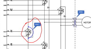
The customer shorted the drain-source of the FET in the lower stage of the U phase (A phase of IC ) and confirmed the operation of MOSFET Overcurrent Protection (VDS_OCP).

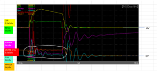
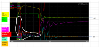
The IC did not detect a short circuit even though the voltage of VDRAIN-SHA exceeded the threshold value of 155 mV for 20us.(Refer to the "Waveform" sheet in the attached Excel)

What is the cause of this?

For register settings, refer to the "Control Register" sheet in the attached Excel.

VDS_OCP.xlsx

Regards,

kura

  • Hi Kura-san,

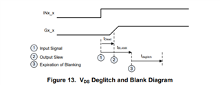
    TBLANK and TVDS are 1.75us in the registers, so this is at least 3.5us until VDS can be detected. 

    In the circled region below, it appears VDS is switching and not stable until around 5us after INHA transitions high. Can you increase TBLANK to 3.5 or 7us?

    VDS should be tripping after the TBLANK period. After a trip is detected, the TVDS deglitch time of 1.75us must elapse and the trip must still be detected for a VDS overcurrent event to cause latched shutdown. Can you reduce TVDS to 0us to see if this helps after the blanking time is ignored?

    The PCB may not have enough supply or local bulk capacitance for SHx and VDRAIN to switch current fast enough when the short is introduced. There is lots of ringing at VDRAIN and SHx when the short is introduced. Can you try the test with lower currents to see if ringing or overshoots/undershoots to see if VDS voltage not being monitored correctly? Also measuring VDRAIN-SHx voltage at the FETs rather than test points may help with improved measurements. 

    Thanks,
    Aaron

  • Aaron-san

    Thank you for your support.

    We got following information from customer.

    VDS_OCP did not work when TBLANK was 7us.
    VDS_OCP worked when TVDS was set to 0us.
    This was confirmed at 6V, 12V, 16V.

    The customer wants to confirm the following two points.

    1. Is there a limit to the VDRAIN voltage for VDS_OCP to work?
    For example, if the VDRAIN voltage drops from 10V to 1V, will VDS overcurrent cannot be detected in the circuit or will the detection threshold be raised?

    If there is a limit to the voltage of VDRAIN, please tell me how many volts VDRAIN can detect overcurrent as intended.

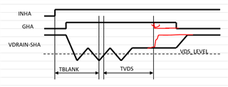
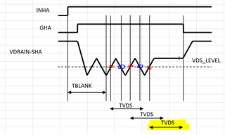
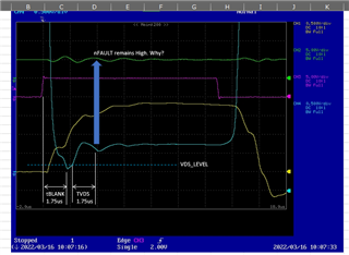
    2. Does VDS_OCP detect a short circuit if the ringing continues for more than the TBLANK period and converges at a voltage above VDS_LEVEL as shown in the attached figure?

    1614.waveform.xlsx

    Please advise us.

    Regards,

    Kura

  • Hi Kura-san

    Good to hear TVDS = 0us worked. 

    1. Is there a limit to the VDRAIN voltage for VDS_OCP to work?
    For example, if the VDRAIN voltage drops from 10V to 1V, will VDS overcurrent cannot be detected in the circuit or will the detection threshold be raised?

    VDRAIN is rated from -0.3V to 45V, so there should not be a limit if it's in that range. The only rule to VDS OCP monitoring is that when the associated input is high is when VDS OCP is monitored (after TBLANK elapses). 

    2. Does VDS_OCP detect a short circuit if the ringing continues for more than the TBLANK period and converges at a voltage above VDS_LEVEL as shown in the attached figure?

    In the diagram you showed, TVDS would occur actually at the first instance VDS > VDS_LEVEL after the TBLANK time, as shown below. TVDS is a timer, and does not get interrupted unless if the input changes states. If ringing occurs, the timer would continue to elapse and check the VDS voltage after the time has elapsed, so it does not care if it experiences ringing during the TVDS period. 

    Thanks,
    Aaron

  • Aaron-san

    Thank you for your support.

    We got additional questions 

    Question 1.
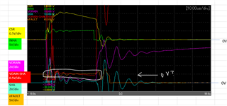
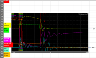
    From the previous answer, the customer thinks VDS_OCP will detect a short in the first waveform(below), but not. What are the possible reasons? 0027.VDS_OCP.xlsx

    Question 2.
    What could be the reason why VDS_OCP did not work with TBLANK set to 7us?

    Question 3.
    If the VDS voltage does not exceed VDS_LEVEL at the end of the TVDS period, will VDS_OCP not detect a short circuit?

    Question 4.
    If VDS_OCP does not detect a short in Question 3, will the TVDS timer start again?

    waveform2.xlsx

    Please advise us.

    Regards,

    Kura

  • Hi Kura-san,

    1) If the labels are correct, then VDS_OCP should have triggered because 0.5V > 0.155V; however, when the high-side FET is switched on, and there is a difference of 0.5V, this means the current going through the FET will be 0.5V/Rdson of the FET. Please check is this is correct with the current of the motor and Rdson of the FET, because usually this should be closer to 0-V if a small Rdson FET is used. 

    If the vertical position is correct, then there may be in accurate measurements if a larger ground loop is used when probing VDRAIN-SHA. The scope should measure the most accurate VDS measurement if the scope probes right at the drain and source of the MOSFET. Inductance from the VDRAIN and SHA traces back to the DRV8305 can also affect the measurement of the VDS monitors. 

    If the measurement is correct, the ringing on VDRAIN-SHA can also be affecting this VDS measurement from the VDS monitor. Can you see if adding VDRAIN-GND bypass/bulk capacitors and tuning RC snubbers on the MOSFET can help with this?

    2) I think it did not work with 7us because the DRV8305-Q1 is seeing the "settled" VDS voltage as under the VDS_OCP threshold. At 0us, there is a much higher voltage that is detected by the VDS monitor. 

    3) This is correct. If the VDS voltage at the end of the TVDS period is not higher than VDS_OCP, then the overcurrent event will not trigger because the TVDS timer is absolute and will only compare the final VDS voltage once the TVDS timer is completed. 

    4) I am not sure actually, I'll need to ask design. My assumption would be yes though because VDS monitoring should be active as long as the input is high, so the timer should be continuously active. I'll confirm in the next couple of days. 

    Thanks,

    Aaron

  • Hi Kura-san,

    I got additional feedback from designer. 

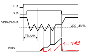
    TVDS will only keep counting as long as VDS > VDS_LEVEL. If VDS < VDS_LEVEL, TVDS will stop counting and wait for VDS > VDS_LEVEL to begin counting again. This means the timer isn't an "absolute" timer, it is conditional and only activates when it detects the potential overcurrent event. 

    Below the red points show when TVDS begins counting, and the blue points shown when TVDS stop counting because VDS < VDS_LEVEL. Only the last instance at the purple point (highlighted VDS time) is when an overcurrent event will trigger. There will be no repeat counting of the VDS timer, unlike previously assumed. 

    Thanks,
    Aaron

  • Aaron-san

    Thank you for your support.

    We got additional questions from customer. Please check below.

    1.They remeasured the waveform. Noise during measurement is reduced.

       The conditions for VDS_OCP to work are met, but it is not detected.

       In addition to the waveform, numerical data and a circuit diagram are also attached because they think it will be useful for investigation

       so that there is no doubt about the waveform. What are the possible reasons why VDS_OCP does not work?

       Also, VDS_OCP did not work even if VDS_LEVEL was set to 0b00000.

    waveform_ data_circuit.xlsx

    2.To summarize your answers, does the TVDS timer behave as shown in the figure below?

    Please advise us.

    Regards,

    Kura

  • Hi Kura-san,

    I need some time for review, I'll reply by end of the week.

    Thanks,
    Aaron

  • Hi Kura-san,

    I have some follow up questions:

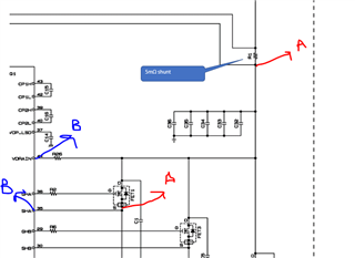
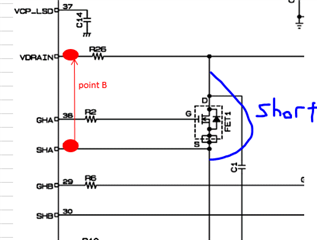
    1) Can you show in the circuit where VDRAIN-SHx was measured? We recommend to measure as close to the DRV IC pins as possible rather than near the MOSFETs because parasitic inductance in the power stage layout can affect the VDS measurements seen by the DRV8305-Q1. 

    For instance, measuring at points A for VDRAIN-SHx can show that the VDS voltage measured exceeds VDS_LEVEL, but measuring at points B can show a different VDS behavior measured by the DRV8305-Q1. 

    2) A way we like to test VDS overcurrent on the bench is removing the MOSFET and applying the literal voltages at the drain and source of the MOSFET. Would the customer be open to VDS evaluation by removing the MOSFET and applying VM and then applying VM - 0.155V at SHx to see if VDS overcurrent trips? Again, parasitic inductances or MOSFET parasitics can affect the actual VDS measurement seen by the DRV. 

    3) When the short circuit condition is introduced, it seems like hundreds of amps introduced. Can the supply handle this condition? It's unlikely, but is it possible the supply browns out below the UVLO threshold and the device does not detect this fault condition because the logic core is not active?

    Thanks,
    Aaron

  • Aaron-san

    Thank you for your support.

    We got more information from customer.


    -It is confirmed that the register is set correctly in the SPI waveform.

    -The attenuation settings for the oscilloscope and probe are the same.

    -The voltage between VDRAIN and SHA and the short-circuit current match.

    ・ Does "Rather than shorting the LS FET's VDS, can you short SH_x to GND and reperform the test on the HS FET to see if this improves VDS OCP?" Mean a short circuit at the IC end?

    Since the pattern at the end of the IC is thin, it cannot withstand short-circuit current. It was

    Is "Does the VDS measurement work better or correctly when INLA = 1 and SH_X-SL_x is monitored?" asked about the case of the upper short?
    If so, VDS_OCP is working in the case of the upper short.

    1) Added measured points A and B to the file.

    waveform_ data_circuit2.xlsx
    2) They think VDS_OCP will work with the proposed method, but that is not a test to see if it works with the system.

        The purpose is not to check the operation of the IC alone, but to check the fail-safe on the mounting board, so it does not meet the purpose.

    3) As shown earlier, P VDD is 6.8V even if dropped.

    Regards,

    Kura

  • Hi Kura-san,

    I'll get you a reply by the end of the week.

    Thanks,
    Aaron

  • Hi Kura-san,

    I reviewed the waveform and I agree it still seems like the trip is not happening correctly still. I have some more ideas for testing:

    - Originally there is a lot of coupling when the short is introduced in other signals, including nFAULT. Can the customer probe EN_GATE and WAKE to see if the device is temporarily going into a different operating state?

    - Can the customer introduce a lower short circuit current to see if ringing is decreased?

    Is "Does the VDS measurement work better or correctly when INLA = 1 and SH_X-SL_x is monitored?" asked about the case of the upper short?
    If so, VDS_OCP is working in the case of the upper short.

    If VDS_OCP works on the high side as below when there is a short across the HS MOSFET, then it is likely the ringing introduced from switching this on is affecting the measurement. Would reducing the IDRIVE setting help?

    Thanks,

    Aaron

  • Aaron-san

    Thank you for your support.

    We received answer for your questions from customer.

    Can the customer probe EN_GATE and WAKE to see if the device is temporarily going into a different operating state?

    ->Due to the advice they received earlier, the WAKE pin is open and cannot be observed because there is no measurement pad.
       EN_GATE remains Hi as long as it is confirmed with an oscilloscope.

    Can the customer introduce a lower short circuit current to see if ringing is decreased?-

    ->VDS_OCP is not working at 6V, 12V, 16V. This is the same as changing the short current.
      (Since I = V / R, if "V" is made smaller, "I" will also be made smaller.)
       At this time, there was no big difference in ringing.

    If VDS_OCP works on the high side as below when there is a short across the HS MOSFET,then it is likely the ringing introduced from switching this on is affecting the measurement. Would reducing the IDRIVE setting help?

    ->In the upper short, VDS_OCP cannot be detected in the upper stage, and when the lower stage is turned on, VDS_OCP is detected in the Vds of

       the lower FET.

       In the upper short, VDS_OCP is working even with our setting value, so I don't think it is necessary to change IDRIVE.
       In the lower short, VDS_OCP did not work even if IDRAIVE was set to the lower limit.

    Below are additional questions.

    6521.waveform_ data_circuit2.xlsx
    (1) You are paying attention to ringing, but does it mean that VDS_OCP is not acceptable even for ringing of attached file?

    (2) Or is there a possibility that the IC will malfunction due to the ringing presented in attached?
    Ringing may appear larger depending on the measurement method, so it may actually be smaller.

    (3) Please indicate the allowable ringing.

    (4)Again, please tell us the possible reasons why VDS_OCP does not work.

    (5)To summarize your previous answers, does the TVDS timer behave as shown in the figure below? Please give us your comment.

    Regards,

    Kura

  • Hi Kura-san,

    I am reviewing the information and will provide you a response tomorrow.

    Thanks,
    Aaron

  • Hi Kura-san,

    I received some feedback from my team members as well to continue investigation. Rather than paying attention to ringing for now, I want to focus on VDRAIN measurement. 

    Since VDS_OCP works on the LS FET when the HS FET is shorted, and VDS_OCP is not working on the HS FET when the LS FET is shorted, the main difference between low-side and high-side measurements is VDRAIN. 

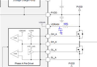
    • Can you share the VDRAIN resistance value used? Is it 100 ohms or less? High resistance can affect VDRAIN measurement. 
    • Is there difference in VDRAIN measurement at the IC pin vs HS MOSFET drain? 
    • Can you share layout of motor driver and powerstage? I want to see if layout of VDRAIN adds inductance in VDRAIN trace and therefore measurement is being affected at VDRAIN. 

    TVDS timer works as shown below. 

    DRV8305-Q1 has been in production for many years so VDS monitors should be accurate. 

    Thanks,
    Aaron

  • Aaron-san

    Thank you for your support.

    We received answer or comment from customer for your questions.

    >Can you share the VDRAIN resistance value used? Is it 100 ohms or less? High resistance can affect VDRAIN measurement.

    --->RVDRAIN is 100ohms +/-5%

    >Is there difference in VDRAIN measurement at the IC pin vs HS MOSFET drain?

    ---->They think there is a difference, but they expect that the IC judges VDS_OCP based on the voltage of the VDRAIN terminal,

          so they think that the VDRAIN terminal voltage is more important than the drain terminal voltage of the FET.

         Or is it predicting the drain terminal voltage of the FET from the VDRAIN terminal voltage?

    >Can you share layout of motor driver and powerstage?

    >I want to see if layout of VDRAIN adds inductance in VDRAIN trace and therefore measurement is being affected at VDRAIN.

    ---->I received layout information from customer. I will send this information to you thru your local FAE.

    >DRV8305-Q1 has been in production for many years so VDS monitors should be accurate.

    ---->They think that's true, but it's also true that VDS_OCP isn't working.

    Regards,

    Kura

  • Hi Kura-san,

    Thanks, I will wait for email from my local FAE for the layout. 

    Does replacing the MOSFET or DRV8305-Q1 have the same VDS results? If the test was performed on another PCB, does it have the same VDS results?

    Thanks,
    Aaron

  • Aaron-san

    Thank you for your support.

    They have not replaced only the FET or only DRV8305-Q1.

    They performed on three boards and all the results are the same.

    I think you received layout information. Please advise us.

    Regards,

    Kura

  • Hi Kura-san,

    I received the PCB layout and will get you a reply tomorrow. 

    Thanks,
    Aaron

  • Aaron-san

    Thank you for your support.

    If you have any update, please let us know it.

    Regards,

    Kura

  • Hi Kura-san.

    I reviewed the layout, I did not see issues with the routing of VDRAIN to the DRV8305-Q1 for high-side VDRAIN measurement. 

    We have a few more theories based on previous waveforms shared:

    1) Can customer share picture of test setup with the short wire? Can the wire support the current of the short circuit?

    The wire can add inductance to the motor current path and we see VDRAIN dips very low, which can be affecting VDRAIN-SHx measurement.

    2) We see from original waveform that VDRAIN dips to almost 0V when the short happens, in which we are not sure if the HS VDS comparator (VDRAIN-SHx) responds when the voltage is this low. There is a difference between PVDD and VDRAIN voltage as well, but since this is less than 10V difference, device should be okay. 

    We are checking with design to see how DRV8305-Q1 VDS comparator is implemented and whether the VDS comparator malfunctions when VDRAIN is near 0V. 

    3) Can the customer share waveforms of the low-side VDS comparator detecting the VDS fault when they short the HS FET's drain-to-source and turn on the LS FET? I want to see if there are any noticeable differences. The main difference is VDRAIN between the two behaviors. 

    Thanks,
    Aaron

  • Aaron-san

    Thank you for your support.

    We got additional information from customer for your question.

    1)

    The length of 0.5mm is solder shorted with a width of about 2mm.

    They think the inductance is small enough to have no effect. Also, They think it can withstand short currents.

    You can see that the parasitic inductance is a concern, but as the waveform shows, the voltage between VDRAIN and SHA is large enough.

    Also, from the answers received so far, they think that even if there is noise (ringing) in the process up to VDS_OCP detection, VDS_OCP will be detected if it finally exceeds VDS_LEVEL.Is their understanding correct? Should they focus on ringing?

    2)

    They think waveform you attached has a measurement flaw and is superposed with noise.

    Please refer to following waveform(This waveform reduces measurement noise.)

    /cfs-file/__key/communityserver-discussions-components-files/38/6521.waveform_5F00_-data_5F00_circuit2.xlsx

    3)

    The measurement noise is large and there is no waveform that can be presented.
    The waveform needs to be retaken, but it is being used in another test and cannot be measured immediately.

    Regards,

    Kura

  • Hi Kura-san,

    I'll provide a reply tomorrow morning. 

    Thanks,
    Aaron

  • Aaron-san

    Thank you for your support.

    If you have any update, please let us know it.

    Regards,

    Kura

  • Hi Kura-san, 

    Some of our team members are currently out for travel 

    But we will review your questions and aim to provide a response soon

    Best Regards, 
    Andrew 

  • Hi Kura-san,

    Apologize as I was out. 

    1) The width of the solder short (~78mil) is concerning as it should not be able to support a large amount of short circuit current (i.e. hundreds of amps) for a transient amount of time. Usually we recommend 10mil width of conductivity for 1 amp of current. 

    2) Understood. That waveform shows the issue clearly. I am still working with design on a minimum amount of VDRAIN-SHx voltage required for the HS VDS comparator to work, there could still be a design condition that is not causing HS VDS to trip correctly because I am still under the impression VDRAIN and SHA brown out to very low voltages near 0V.

    3) Understood. 

    Thanks,
    Aaron

  • Aaron-san

    Thank you for your support.

    If you have any update, please let us know it.

    Customer would like to know the reason why VDS_OCP didn't not work.

    Regards,

    Kura

  • Hi Kura-san,

    Our team is currently still looking into this issue, but I did have a question on the customer's implementation & waveforms: 

    1. From system-level behavior during this short-circuit test & VDS evaluation,
      1. would it be possible to recreate this waveform, and add the signal of VDRAIN voltage w/ reference to GND (0V)? 
      2. May be able to remove Ch1 (shunt resistor voltage to indicate motor current) 
      3. we want to better understand the true profile of VDRAIN at the time of this test, its lowest value during the test, and the specific timing relative to HS VDS voltage differential
    2. do you think it would be possible for the customer to try and stabilize VDRAIN DC-bus voltage during this s.c. test? 
      1. e.g. add more bulk capacitance (many hundreds of microFarads) to prevent VDRAIN from decreasing too quickly 
      2. e.g. add more bypass capacitance (small 0.1uF, 1uF type capacitor values in parallel to help filter out high-frequency noise)
      3. our team is interested to understand if the customer's results will differ with VDRAIN voltage  

    VDRAIN waveform is indeed present here, but time scale is a bit too large to evaluate closely: 

    Best Regards, 
    Andrew 

  • Hi Kura-san,

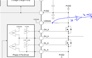
    To provide some closure to this issue, because VDRAIN drops below PVDD_UVLO1 (4.1V) during the high-side VDS overcurrent test, and the expectation is VDRAIN is tied to PVDD with a 100-ohm resistor, the VDRAIN monitor will not function normally in design as the VDRAIN monitor needs to be above PVDD_UVLO1. For the high-side VDRAIN-SHx monitoring to work, VDRAIN should remain

    Therefore, we would like to propose 2 workarounds:

    1) Place a capacitor from VDRAIN-GND between the VDRAIN pin and 100-ohm VDRAIN resistor to help maintain VDRAIN above the PVDD_UVLO1 level. 

    2) Implement external monitoring on VDRAIN so that when VDRAIN dips to the voltage seen during the short circuit test (~1-2V), register this event as a VDS overcurrent event. 

    Thanks,
    Aaron

  • Aaron-san

    Thank you for your support.

    Our customer has following additional question.

     About register reset:
    They think that all registers will be reset when PVDD falls below PVDD_UVLO1, but is it possible that some registers will be reset and some will not be reset if the voltage drops momentarily when PVDD drops?

    Or, if a particular register is reset, is it safe to assume that other registers are also reset?

    Also, if all registers are always reset, please let us know the reason why?

    (For example, if PVDD falls below PVDD_UVLO1, the circuit that positively resets the register will operate.

    Please advise us.

    Regards,

    Kura

  • Hi Kura-san,

    When PVDD < PVDD_UVLO1 for greater than 8-10us, all SPI registers will be reset as internal logic is disabled. 

    Before 8us, the registers should not lose any contents. I cannot comment on whether registers will be partially reset or fully reset if the undervoltage happens between 8-10us.  

    Thanks,
    Aaron

  • Aaron-san

    Thank you for your support.

    Our customer has following additional question.

     About the low voltage protection threshold of the charge pump:

    The customer believes that if the charge pump low voltage protection threshold setting is set to SET_VCPH_UV = 0V, the protection function will work at Max 5.3V.

    Is it okay to assume that the charge pump normally does not drop to 5.3 V (= the charge pump's low voltage protection does not work) within the range of PVDD = 4.4 to 45 V?

    Please see attached.file.xlsx

    The MIN value of the Vgs guaranteed voltage of the high side gate driver is 5V.
    The customer would like to check if the charge pump low voltage protection can still work or not work within the range of P VDD = 4.4 to 45 V.

    If there is a working case ,please let us know it.

    Regards,

    Kura

  • Hi Kura-san,

    Is it okay to assume that the charge pump normally does not drop to 5.3 V (= the charge pump's low voltage protection does not work) within the range of PVDD = 4.4 to 45 V?

    The specification in the register setting is 4.9V typical for SET_VCPH_UV = 0V, which assumes that the VGHS is at minimum 5V. 

    I need to check with systems today what the likelihood of VVCPH_UVLO2 = 5 to 5.3V is in this device, since this overlap is indicating that SET_VCPH_UV may trip at 5 to 5.3V even though VGHS can be as low as 5V w.r.t. PVDD. 

    Thanks,
    Aaron

  • Hi Kura-san,

    According to characterization data, the VGHS value did not show it dropping below 5.9V, but the spec in the datasheet is normally assumed to be six sigma deviation, so this is why VGHS = 5V beyond the characterization data.

    The HS Vgs is generated independently of the VCPH_UV threshold. The UV threshold will vary based on the specifics of the bandgap and threshold voltage reference, while the Vgs will be more dependent on the temperature and process variation of the FETs in the charge pump.

    The datasheet implies that the purpose of the SET_VCPH_UV = 1 mode is specifically to ensure that VCPH_UV does not trigger if the device may potentially drop below 5.3V VCPH in the 4.4 to 5.5V operating condition. It feels like less of a conflict and more of a reason why we have these two different thresholds.

    Thanks,
    Aaron