Hi team,
Here're some issues from the customer may need your help:
Q1: What is the purpose of a loop that requires an additional LPF on the PWM control loop? In a design, what is the principle if the filter capacitance of PWM+ is removed and it is prone to pull the INTZ low (overcurrent protection) causing the drive IC to not operate?
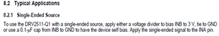
Q2: In the case of single-ended inputs, the INB is handled in three ways, what are the differences and how to choose them?
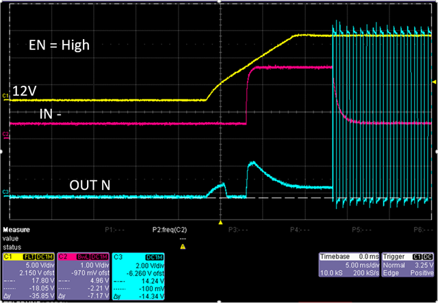
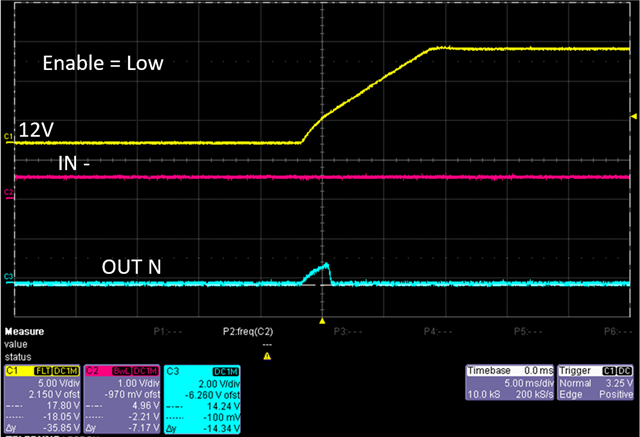
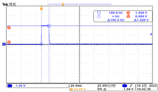
Q3: When the power supply is powered up, the IC itself generates a PWM pulse of 10 ms. Why is that?
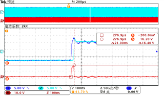
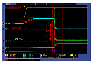
Q4: When out+ rises from 0 V to 6 V during power up, a pulse is generated, why is this pulse generated? How is this pulse filtered out?
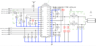
And the schematic is as follows:
Could you help check this case? Thanks.
Best Regards,
Cherry