This thread has been locked.

If you have a related question, please click the "Ask a related question" button in the top right corner. The newly created question will be automatically linked to this question.

DRV8302: DRV8302 heats up on giving power, AVDD, GVDD, and buck output are all at 0V.

Part Number: DRV8302

Hi everyone,

I am working on a BLDC motor controller design using DRV8302. I am having problem with DRV8302 because it heats up as soon as i turn the 24V supply. I have measured voltages at AVDD, GVDD and Buck output pins, they are all at 0V. What should i test first?

I am not sure whether i have purchased a genuine DRV8302 or it's counterpart. Here is the Part number(94C9H9TG4 DRV8302) of DRV8302 that i have purchased, Please someone verify it's genuine or not.

Thanks.

  • Hi Mohammad,

    Thank you for posting your question to the motor drives forum! I have a few questions to see if I can better understand the issue.

    1. Are you using a custom PCB that you are soldering the DRV8302 onto? If so, could you provide the schematic to see if there could be anything from the design that could cause this behavior? It sounds like there may be a short/low impedance to ground that might be occurring, or the supply voltage may not be being applied to the correct pins. 

    2. Have you observed this issue on multiple devices on multiple boards? Does this happen on brand new boards with brand new devices? Has there been any instances where you have been able to successfully power up the device?

    Regards,

    Anthony Lodi

  • Yes, i am using a custom PCB. Please find the schematic attached below.

    Yes, i have observed this issue on multiple devices on multiple boards. It happens on new boards as well.

    It worked only once, but only output waveform was available on one channel.

    Thanks.

  • This is the behaviour of AVdd (Ch1- yellow) Gvdd (Ch2-purple) for 2 drv8302 IC's soldered on the same board (Ch3-blue & Ch4- green correspond to the second IC.

  • Never mind this, it was just switch bouncing on the input. GVdd AVdd and PVdd never turn on. Also nFault and nOctw are high on both ic's (no fault or overcurrent condition)

  • Hi Mohammad,

    There was nothing in the circuit that I saw that seemed concerning from a schematic point of view. Could you measure the voltage at the PVDD1 and PVDD2 pins? I want to see what is happening at the input. Can you verify that the component was not soldered on backwards in orientation? Could you start up the device with EN_BUCK low just in case the issue is related to the buck? 

    Regards,

    Anthony Lodi

  • Hi anthony, talha here. Me and Mohammed are working together on this project. We have disabled buck completely (En-Buck connected to GND) just in case the regulator was causing these issues. PVDD1 is 24V and PVDD2 is 24v as well. I'm attaching images of our design here for your reference perhaps something in the pcb layout is obviously wrong or not standard?

    Pin1 is bottom left 

    Top layerIn1In2Bottom layer

  • Hi Talha,

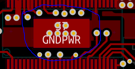
    Nothing stands out to me as obviously the issue when looking at the layout. Are the vias tented? I could see a scenario where a solder bridge could be occurring between the GND pad of the DRV and the vias that are near the ground pad if the vias are not tented.

    Can you measure how much current is being consumed by the device after power on? is the voltage at the DVDD pin also 0V? Or is it outputting 3.3V? 

    Could you send a good quality picture of the IC on your board to see if I can see anything that could be a problem from the physical connections? You could also try to measure the impedance between the PVDD pins and GND to see if there is a low impedance path. 

    One side note is that I wouldn't recommend putting the CP1-CP2 capacitor on the bottom of the board, since this results in added inductance in that path since it has to go through 2 vias which can negatively impact the performance of the trickle charge pump. 

    Regards,

    Anthony Lodi

  • Hi Talha,

    Do you need assistance on this thread still? If not, please mark as resolved!

    Thanks,
    Aaron

  • The problem was with the EN_GATE pin. When this pin is set to high all the voltages GVDD, AVDD, and PVDD appear, although EN_GATE pin is only responsible for enabling the gate of driver and current shunt amplifier.

    Thanks.