Because of the holidays, TI E2E™ design support forum responses will be delayed from Dec. 25 through Jan. 2. Thank you for your patience.

This thread has been locked.

If you have a related question, please click the "Ask a related question" button in the top right corner. The newly created question will be automatically linked to this question.

DRV8662: Drives two cascaded piezo ceramic

Part Number: DRV8662
Other Parts Discussed in Thread: DRV2700

Hi team

Here're some issues from the customer may need your help:

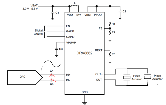
1) In actual applications, a piezo deflection mirror with two cascaded piezo ceramic whose length difference determines the angle of the platform they support after applying different voltages. Each piezo ceramic is polarity-driven and the negative voltage cannot be higher than the positive voltage. Can this chip guarantee that OUT+ is always greater than OUT-?

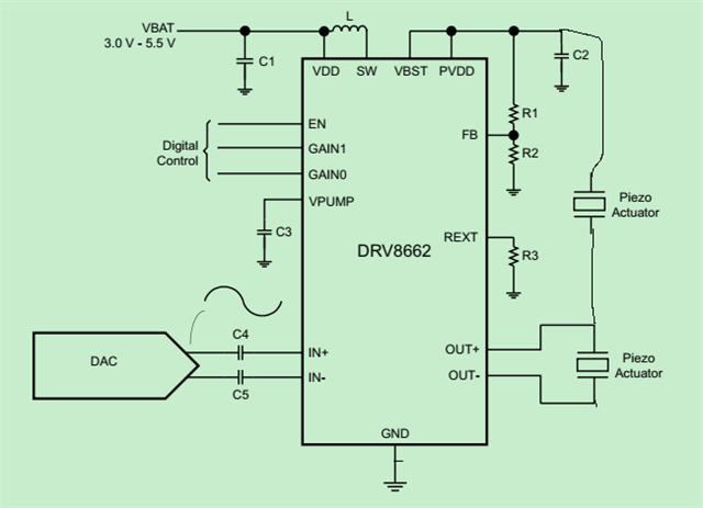
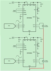
2) Can the two piezo ceramic that have been cascaded be driven as following figure? The next set of OUT- terminals is connected to ground and its OUT+ is connected to the OUT- side of the previous set. The effect is that for the following group, OUT- is fixed to GND, and for the above group, OUT- is followed by OUT+. The manual does not seem to mention whether or not the voltage of OUT- can be specified. Dose it have to be floating as shown?
3) And regarding the following 4 threads, which are confusing, can input be a DC signal that keeps the OUT voltage in a constant state?

DRV8662: Coupling capacitor - Motor drivers forum - Motor drivers - TI E2E support forums

DRV8662: Single-ended DC operation - Motor drivers forum - Motor drivers - TI E2E support forums

DRV8662: input signal form for DRV8662 - Motor drivers forum - Motor drivers - TI E2E support forums

DRV8662: Driving a Piezo Stack with a unipolar low frequency pulse (rectangular infrequent signal input), DRV8662 vs DRV2700 - Motor drivers forum - Motor drivers - TI E2E support forums

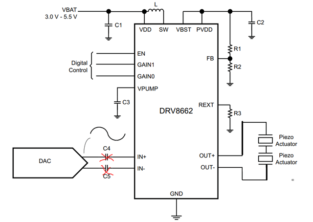
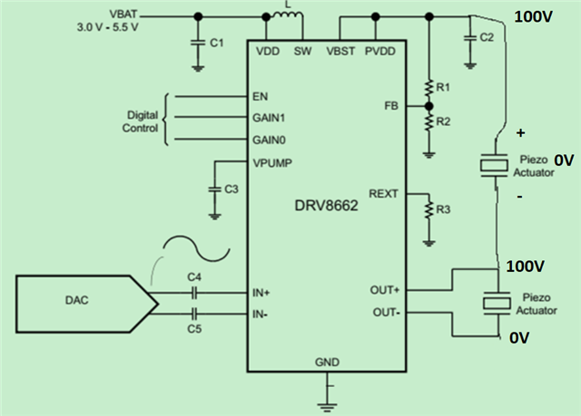
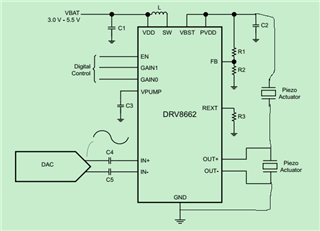
4) Is it possible to drive two cascaded piezo ceramic as shown below? The total voltage of the two piezo ceramics is constant at, for example, 100 V.
5)a. What is the duty cycle of the output voltage versus the PWM signal if a PWM input is used?

b. How does the drive chip identify whether it is a PWM signal or an analogue signal? Or is it that the drive chip does not recognize, and the external filter of the chip will smooth the PWM signal into an analogue signal?

c. If IN+ is greater than IN-, is OUT+ greater than OUT-?

Could you help check this case? Thanks.

Best Regards,

Cherry

  • Hi Cherry,

    Apologize for the delay I will give my response later this week

    Regards,

    Arthur

  • Hi Arthur,

    Thanks and expect the response.

    Thanks and regards,

    Cherry

  • Hi Cherry,

    Sorry for the delay here. I needed to order DRV8662 EVM in order to test this.

    I will give my thoughtful response tomorrow

    Regards,

    Arthur

  • Hi Cherry

    In actual applications, a piezo deflection mirror with two cascaded piezo ceramic whose length difference determines the angle of the platform they support after applying different voltages. Each piezo ceramic is polarity-driven and the negative voltage cannot be higher than the positive voltage. Can this chip guarantee that OUT+ is always greater than OUT-?

    the output will be in phase with the input. If in+ is higher than in- then out+ will be higher than out-

    Can the two piezo ceramic that have been cascaded be driven as following figure? The next set of OUT- terminals is connected to ground and its OUT+ is connected to the OUT- side of the previous set. The effect is that for the following group, OUT- is fixed to GND, and for the above group, OUT- is followed by OUT+. The manual does not seem to mention whether or not the voltage of OUT- can be specified. Dose it have to be floating as shown?

    You cannot connect OUT- directly to GND. the piezo can be connected in series to achieve up to 50V DC across both, or then can be connected in parallel to achieve 100V across both.

    And regarding the following 4 threads, which are confusing, can input be a DC signal that keeps the OUT voltage in a constant state?

    Yes, when the inputs are DC coupled(NO DC blocking capacitor)

    Is it possible to drive two cascaded piezo ceramic as shown below? The total voltage of the two piezo ceramics is constant at, for example, 100 V.

    No, you cannot connect OUT- to GND. In addition to this the voltage difference between PVDD and OUT+ will not be 100V. it will be close to 0V.

    a. What is the duty cycle of the output voltage versus the PWM signal if a PWM input is used?

    the output is an amplified copy of the input signal. The input should also be filtered if it is PWM. It is not recommended to use a direct PWM connection.

    How does the drive chip identify whether it is a PWM signal or an analogue signal? Or is it that the drive chip does not recognize, and the external filter of the chip will smooth the PWM signal into an analogue signal?

    "Or is it that the drive chip does not recognize, and the external filter of the chip will smooth the PWM signal into an analogue signal?" - this is correct

    c. If IN+ is greater than IN-, is OUT+ greater than OUT-?

    Yes

    Regards,

    Arthur

  • Thank you for the detailed explanation

    I am the customer mentioned by Cherry.

    "You cannot connect OUT- directly to GND. the piezo can be connected in series to achieve up to 50V DC across both, or then can be connected in parallel to achieve 100V across both."

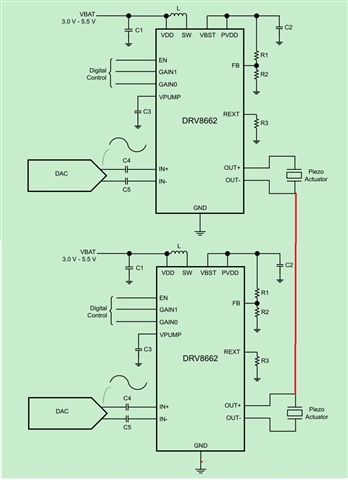
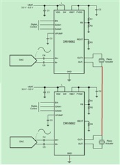
    1) Do you mean in the following connection, the piezo can be connected in series to achieve up to 50V DC across both?  Is this usage recommended? 2) Do you mean if I remove the red wire, then can be connected in parallel to achieve 100V across both? If I do not remove the red wire (which is exists in the products), they are in cascaded connection, not a parallel connect.

    "No, you cannot connect OUT- to GND. In addition to this the voltage difference between PVDD and OUT+ will not be 100V. it will be close to 0V."

    Now I disconnect OUT- with GND in the following figure. Do you mean the piezo will be applied close to 0V in this case? 

  • Hi Xiang,

    I think that I misunderstood the actuator in my previous reply. You need to drive cascaded piezos with a DC voltage. and the voltage on the piezos can never be negative

    1) Is my understanding correct?

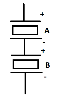
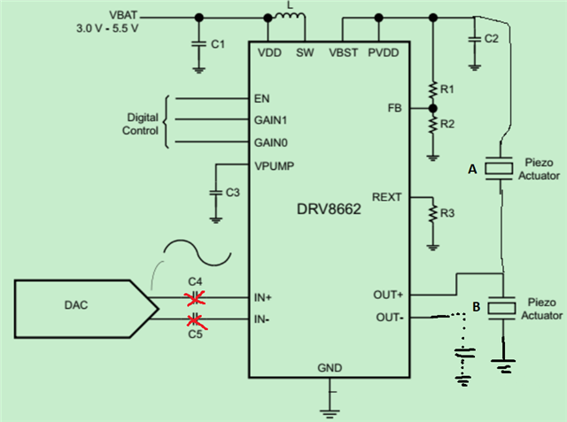
    2) will the voltage across the piezos (I am calling them A, and B) be the same? or will you need different voltages across them. for example 70V on A, and 90V on B?

    When I said 50V in series or 100V in parallel this is what I mean;

    If my understanding is correct then I do not think that DRV8662 is suitable to drive this actuator. the maximum DC voltage that can be generated by this part relative to GND is 105VDC. this part will not be able to drive 100V across two piezo in series because that would require a 200V to GND DC.

    from your example;

    If you need higher than 100VDC, you should consider https://www.ti.com/tool/DRV2700EVM-HV500 This reference design is able to achieve up to 500VDC, and it may be a possible solution in this case.

    Regards,

    Arthur

  • "You need to drive cascaded piezos with a DC voltage. and the voltage on the piezos can never be negative"  This is what I mean.

    "will the voltage across the piezos (I am calling them A, and B) be the same? or will you need different voltages across them. for example 70V on A, and 90V on B?" Yes

    I do not the hope to get 100V on A and 100V on B. I hope the sum of voltage on A and voltage on B is a constant 100V. For example 30V on A and 70V

    on B.

    Do you think the following connection can satisfy this need? Why? 

  • Hi Xiang,

    Thank you for your explanation I now understand the application. 

    these connections will work for your application. the Sum of the voltage across A, and B is always 100V, and the OUT+ terminal can be driven to any DC voltage between 0V-100V.

    the OUT- terminal isn't used, and should be connected to GND with a small capacitor (~1nF @ 100V)

    I just tested this on an EVM in the lab and it works.

    Regards,

    Arthur

  • If the VBST has already established, assume the OUT+ is in a process of rising from 0V or 100V. In the meantime, the Piezo B is charging and the Piezo A is discharging. A will source current to VBST, Is this allowed?

  • The current being sunk by the VBST should not be an issue. the Capacitor C2 should decouple any voltage spike seen on VBST. The absolute max on the VBST is 120V.

    Regards,

    Arthur

  • Thank you. The question is well resolved.

  • I have further question.

    " The boost output voltage may be programmed as high as 105V. A capacitor with a voltage rating of at least the
    boost output voltage must be selected. Since ceramic capacitors tend to come in ratings of 100 V or 250 V, a
    250 V rated 100 nF capacitor of the X5R or X7R type is recommended for the 105 V case. The selected
    capacitor should have a minimum working capacitance of at least 50 nF
    "

    C2 is 0.1uF normally. Is it large enough to decouple any voltage spike seen on VBST?

    @Arthur Brown

    Thank you

  • Hi Xiang,

    As I understand your application will be operating near DC. therefore not much current will be drawn from VBST. A 100 nF 100V or 250V capacitor should be sufficient. If you wish a 1uF capacitor can be used. there will not be an issue increasing this capacitor.

    Regards,

    Arthur

  • Thank you so much

    Each piezo in the application is 0.8uF. Is 0.1uF sufficient?   The voltage  tolerance of the decouple capacitor should be 150 uF considering the boost voltage is 105V,  If I use 1uF capacitor, can I easily find a regular capacitor whose voltage tolerance meets this requirement?

    I think there is a possibility that 0.1uF is sufficient, because in normal operation, when Piezo B is charging, Piezo A is discharging. the current discharges from Piezo A may flow to Piezo B though the DRV8662 from VBST pin? and when B is discharging and Piezo A is charging, the current discharges from Piezo B may flow to Piezo A though the DRV8662 from OUT+ pin? Is this guessing correct?

  • Hi,

    I think that it is possible to find a 1uF capacitor with a voltage rating higher that 105V. I found a few by searching mouser.com

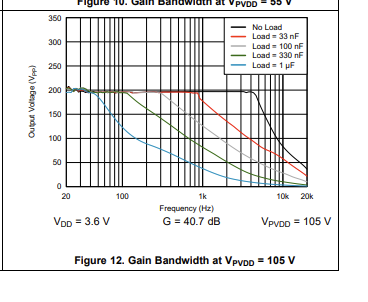
    The DRV8662 shares the same boost architecture as DRV2700, and in the DRV2700 datasheet the gain bandwidth for 1uF load 105V VBST is ~40 Hz. I know that these plots where collected with 0.1uF boost capacitor. So for your application 0.1uF should be able to handle the current needed,

    I think that your guess is correct, when piezo B charges and  A discharges, that charge will flow to VBST node and then through the device into Piezo B.

    When Piezo B discharges I do not think the charge will flow through the device into piezo A. I assume, that it will be sent to GND and dissipated in the device as heat,

    Regards,

    Arthur

  • Thank you.

    We reach a good agreement.

  • Thank you,

    I will close the thread, if any more issues arise you can open a new one and link to this original.

    Regards,

    Arthur