This thread has been locked.

If you have a related question, please click the "Ask a related question" button in the top right corner. The newly created question will be automatically linked to this question.

DRV8353: The device fails when the sink/source currents are increased

Part Number: DRV8353

Hi Team,

We received this inquiry from our customer.

We are having problems with DRV8353 IC can you help?

Problem is IC fails when we increase sink source currents

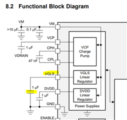
VGLS voltage fails and does not drive low side mosfets

We were using 150ma-200ma for high and low side. For a year there was no problem.

After we increased it to 300ma-600ma motor run for few minutes and we got VGLS UV error

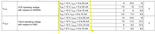
We measured VGLS and it was 4.1V

Then it recovered to11V, cleared error

But not when we try to drive motor we get MOSFET drive error from Low Side MOSFETS

When we scope it we can easily see high side works but no change at low side. I cannot drive low side.

Motor specifications: 48V 350W BLDC, 20 pole pair.

Phase current was around 12A I assume during that few minutes.

Regards,

Danilo

  • Hi Danilo, 

    Thanks for reaching out via the e2e motor drivers forum, and appreciated on the good scope of details provided,

    I think I have a decent idea of what's causing the problem from this info - see below:

    • HS pre-driver uses VCP as overdrive voltage supply to turn on HS MOSFET
    • LS pre-driver uses VGLS as overdrive voltage supply to turn on LS MOSFET 
    • Therefore, if your VCP or VGLS voltages are compromised (e.g. undervoltage that you observed on VGLS),
      • then it will have a direct impact on your gate-drive capabilities for HS and LS respectively
      • and you'll also see a UV fault if it falls significantly enough (e.g. below UV threshold spec) 

    Now as for what the likely root-causes are: 

    1. capacitor value, voltage/temperature rating, and PCB layout (especially for VGLS) 
      1. these caps need to follow datasheet value in functional block diagram,
      2. be rated for 1.5x-2x the voltage they experience (target 16V or higher for VGLS) to avoid de-rating the effective capacitance 
      3. and also be on same-layer as DRV IC, placed very close to the DRV IC pin, and have good thick traces (10-15 mils or more) with no vias in between to give the DRV IC a good signal path 
    2. PCB layout between DRV and MOSFET power stage
      1. to avoid the impacts of parasitic inductance and parasitic capacitance, 
      2. need to place MOSFET power stage connections close to the DRV
      3. target same layer, no vias in between, and 15-20 mils trace thickness. 
    3. VM supply voltage 
      1. Your VDRAIN might be 48V to support motor, but what is VM in your case? 
      2. VM voltage has an impact on VCP/VGLS gate-drive current loading capability, since these regulators use VM to operate 
      3. if your VM is excessively lower than your gate-drive current demand, then you'll see the charge on these regulators deplete under heavy load

    The above 3 points can impede the ability of these regulators to generate the charge needed to maintain gate-drive voltage. 
    This issue gets worse as your IDRIVE setting for source/sink current (since more current will pull charge from VCP/VGLS at higher rates)

    Link to Layout App Note: https://www.ti.com/lit/an/slva959b/slva959b.pdf

    Capacitors for VGLS, VCP, CPH/CPL are all critical for gate-driver overvoltage supplies for HS and LS FETs:

    Gate-drive current loading capability: scales with VM voltage 

    Best Regards, 
    Andrew