This thread has been locked.

If you have a related question, please click the "Ask a related question" button in the top right corner. The newly created question will be automatically linked to this question.

DRV8320: Rare driver failure and weird looking Gate waveforms.

Part Number: DRV8320

Hi, 

I have a bldc design witch is using the DRV8320H. 

Everything works as expected but on some rare occasions, the Driver together with a shot thought happens.

The instances when this happens are at a high current 30-40A close to 100% duty PWM and rapid variations from 70-100% duty.

The device is with Idrive tied vdd so that means 1A with 2A. Wonder if this might be a motive to worry about... the fets would work with lower.

I had 2 such failures where the driver exploded current seemed to flow somehow between a Low side Gate (trace broken by current) and VCP (the VCP 1uf cap was carbonized).

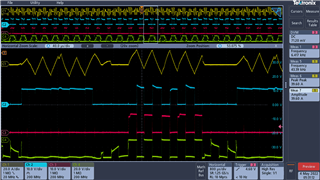
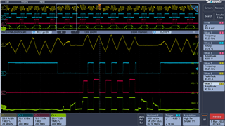
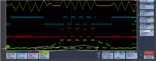
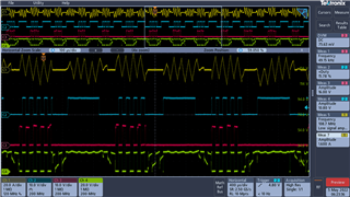
I did not work myself with a smart driver until now so I am not that familiar with it. But after having these problems I started investigating waveforms and I noticed that the Low and High sides look funky.

My SLx pins are connected to common Ground and IDRAIN to VM and OVCP is off. (implemented on the MCU based on current read on low side Sources)

Any hints would ve very much appreciated.

Gabriel

  • Hi Gabriel,

    Please use a lower IDRIVE setting. You are using the max IDRIVE setting which is causing rapid switching of the FETs. Switching high currents very quickly can cause shoot through events from voltage coupling into the LS FET's gate waveform (dV/dt coupling). 

    Here are some resources to understand IDRIVE current selection:

    E2E FAQ on IDRIVE selection: https://e2e.ti.com/support/motor-drivers-group/motor-drivers/f/motor-drivers-forum/796378/faq-selecting-the-best-idrive-setting-and-why-this-is-essential

    System Design Considerations for Higher Power Motors - https://www.ti.com/lit/pdf/slvaf6

    Understanding Smart Gate Drive - https://www.ti.com/lit/pdf/slva714

    Thanks,
    Aaron

  • I have switched the Idrive to the hi-z cause it was the easiest to test out. From calculations, I would need around 85mA so I guess 120mA is ok. 

    The LO gate waveform now looks normal but I am still concerned about the HI gate waveform is this a normal thing to see ?

    Thank you 

  • Hi Liviu, 

    The high-side gate waveform looks better. VGS between GHx-SHx (C3-C4) should be correct if you were to measure these differentially. 

    I can't tell if C4 (which I'm assuming is SHx) is going negative for long amounts of time. If so, this indicates there may be inductance in the power stage or not a good ground return path for motor current.

    Do you have schematic/layout to look over if this is on your own board?

    Thanks,
    Aaron

  • My measurements are like this: 

    c1- current probe

    c2 - Low VGS

    c3 - High VGS (differential probe) 

    c4 - SHA Differential probe Between the Highside source and drain. I had the probe set up on AC. But I noticed no negative voltage.

    so my weird waveform is the high-side gate signal. VGS. It seems to vary in amplitude from 11 to 15V.

    What I noticed though is that if my VM is up to 15v the high side gate signal looks normal in every regard. 

    As I increase the voltage of the system  from 15 up to 25v (max design voltage) the high side waveforms start to vary in voltage quite a lot.

    Still everything works ok. But how could I reduce that variation ?

     Thanks. 

  • Hi Liviu,

    My recommendation is to try and cut the IDRIVE trace and connect it with an 18k/75kohm resistor to GND or connect to GND directly to evaluate lower IDRIVE settings. In the schematic you sent me, connecting it directly to VDD forces your application to operate at the highest IDRIVE setting. Secondly your FETs in your application have a Qgd of 3.8nC, so in order to switch the VDS slew rate at 200ns or slower, I would recommend 3.8nC/200ns = 19mA of gate drive current. 

    You are currently using 1A/2A source/sink currents, or if Hi-Z, 120mA/240mA. The lowest setting is IDRIVE = AGND, which is 10mA/20mA source/sink. This will be better since your FETs are very low Qgd. 

    By using too high of a gate drive current, this can cause Vgs values to be affected. It also depends on your layout, if your gate drive traces are too long or thin, it may not be able to support high IDRIVE currents and cause an increase in voltage because of the increase in inductance (V = L di/dt). 

    Thanks,
    Aaron

  • Thanks,

    all very nice points and I thought about them too. But Why is the High side waveform varying so much when I have a higher VM? If I power the system with let's say 12V the high side looks identical to the good low side waveform if I go past 15v VM that strange waveform appears. Just want to be sure I am on the safe side with it. My traces are very short 0.2mm 2oz. Anyway, thank you very much for the help, Aaron!

    Liviu

  • Hi Liviu, 

    As VM increases, IVCP and GHx increases to around 11V. 

    But looking at SHx, there is a -3 to -4V when SHx goes low. 

    Differentially this seems to be causing VGS to go 3 to 4V higher than expected as you see on your waveform, as if the ground reference for the high side gate is too low. 

    Can you confirm that the measurement is taken for VGS and SHx near the IC pins and not the FETs? 

    If the -3V to -4V still appears at SHx when the low-side FET turns on, there may be impedance in the grounding or the switch node path through the LS FET to GND has a lot of impedance. If there is 0.1ohms of impedance in the motor current path, then this can be causing the 30-40A * 0.1ohms to generate -3V to -4V at SHx. 

    Could you share layout?

    Thanks,
    Aaron

  • hi, I am attaching the new measurement. The SHx pin is taken from the switch node of fets the distance between that point and the IC pin is like 10mm max.

    Liviu

  • Hi Liviu,

    I think your SHx measurement is inverted. Does increasing the PWM frequency help? I think you're using 5kHz or 6kHz PWM frequency which is pretty low. 

    Could you share layout over personal message? 

    Thanks,
    Aaron

  • The PWM is 40+ kHz. This capture was at ~50% throttle that's why it looks like this. No matter the layout I have an old layout made by someone else witch was totally different than my current layout but based on the schematic I've sent you(except IDRIVE now I connected it to AGND with 18k. The variation in high side gate voltage happens on both layouts when VM gets over 15v. So my main question is why this is happening, is it a normal thing to see on this device?

    I have stabilized the ringing and slew rates by modifying the IDrive 30-60mA gives me the best results, 10mA barely closes the fets. for 30mA I have ~150ns slew and for 120mA as a comparison I have ~40ns. I would have like 85mA but the HW device jumps from 60 to 120. where I have a slight ringing happening. Leaving that thing aside

  • Hi Liviu,

    This is okay from device operation as there is a 15-V Zener diode clamp from GHx-SHx internally in the driver to prevent the high side FET gate voltage from going over 15-V.

    Is there a common GND used on the PCB? If so, can you ensure the ground between the driver PGND and supply does not have impedance or voltage difference between the two grounds?

    Similarly with the low-side source SLx and GND, can you ensure that there is no impedance between SLx and GND for each phase output to ensure that when GLx is on that SHx is pulled to GND instead of -3 or -4V?

    Thanks,
    Aaron

  • Hi Aaron,

    So, that variation in voltage on the High side gate signal is expected behavior.

    The schematic as you have seen has SLx connected to PGND (close to IC). But my low side fets sources are going through a sense resistor to GND so don't know if the SLx pins are better connected at the sources or gnd as they are now. The shunt is 0.001 it will have a minimal drop but it will be. 

    PGND is connected through a few vias under the IC to the main GND plane (3oz). 

    Other than that I don't know. 

    thank you, 

  • Hi Liviu, 

    It is okay behavior but ideally should be driving around 10-11V above SHx when the HS FET is on. 

    Can you check VCP voltage with respect to VM and see if this is consistently VM + 10V? If it increases, then VCP could be the source of your high-side gate drive issues.

    I missed the fact that SLx on the schematic is connected to PGND. This should be connected to the low-side FET's source, not PGND. The gate current return path and VGS monitoring for the low-side FETs requires SLx to be connected to the low-side source of the FET. 

    Thanks,
    Aaron