This thread has been locked.

If you have a related question, please click the "Ask a related question" button in the top right corner. The newly created question will be automatically linked to this question.

DRV8353: Fault condition swithcing from one to another state in "synchronous 1x PWM" mode

Part Number: DRV8353

Hello!
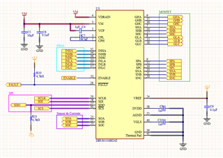
We're facing some problems with the DRV8353SRTAT.
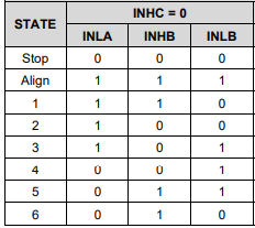
When in "synchronous 1x PWM" mode, as shown in the register table below, a fault ocurrs when changing from any state to another (see the table below):

REG_0x00 0x0
REG_0x01 0x0
REG_0x02 0x40
REG_0x03 0x3ff
REG_0x04 0x7ff
REG_0x05 0x16d
REG_0x06 0x283
REG_0x07 0x0

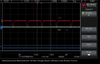
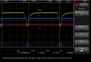
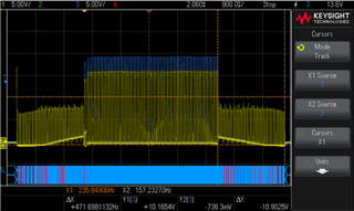
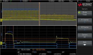
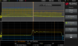
For example, going from "stop" -> 4, with no load attached (only testing signals on the oscilloscope), this change ocurrs well, but sometimes a "gate drive fault on the B low-side MOSFET" occurs. When the change is 4 -> "stop" it aways leads to the same fault (gate drive fault on the B low-side MOSFET) , as registers shown below:

REG_0x00 0x500
REG_0x01 0x4

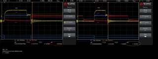
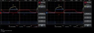
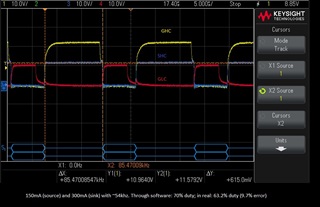
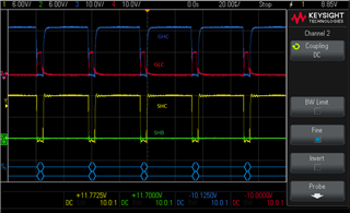
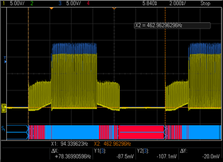
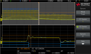
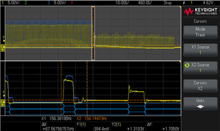
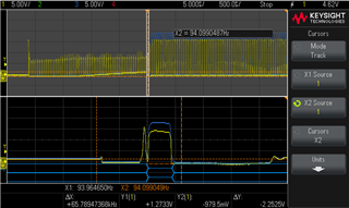
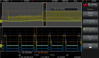
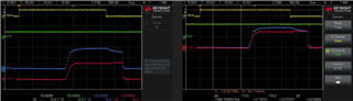
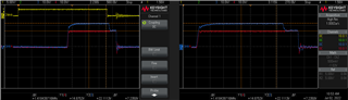
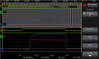
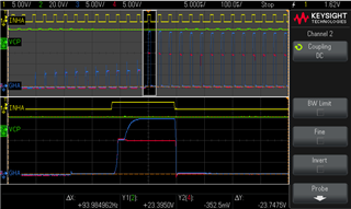
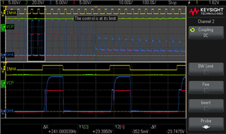
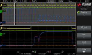
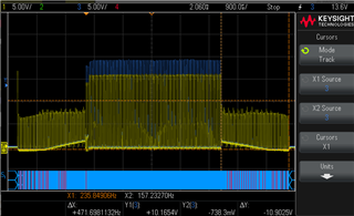
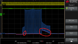
Below, a oscilloscope print of the MOSFET's GHC and GLC signals, as well as Phase C and INHA's PWM signals, where all reference gnd are at the same place as "blue gnd":

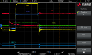
Some importante data:
Voltage: 12v
F ~= 195kHz
Mosfet: IRFS7530 (Qg = 236nC typ.)


If possible, I would like to be enlightened about the following questions:
1- Is this a high Mosfet Qg so that the fault occurs due to this? How to solve this problem? Is it needed to change the mosfets?
2- When transitioning between states on "synchronous 1x PWM", it's expected to be generated a fault? If yes, should we disable "Gate drive Fault" (address = 0x02h)? 
3- What is the maximum recommended Qg and Qgs for the stable functioning?
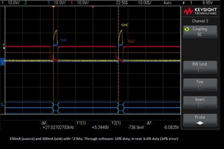
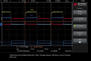
4- Phase C and GHC lower level are both below GND. Is it normal? What does it means?
5- The GLC trace when goes low decays slowly, is this abnormal? What is this ripple at the "low" period?

Best regards and thanks for your help!

  • Hi Emanuel,

    Before answering the questions, first thing we always look for when someone reports a "Gate Drive Fault" is to check the IDRIVE settings. I can see you're using the max gate current settings for switching your MOSFET! The "FF" corresponds to 1-A source and 2-A sink gate current for your MOSFETs. 

    Using too high of an IDRIVE current will slam your FETs on and off really fast leading to potential gate drive faults as inductance in the gate drive traces can generate spiking, transients, or even damage at GHx/GLx. Use a lower IDRIVE setting based on this FAQ: https://e2e.ti.com/support/motor-drivers-group/motor-drivers/f/motor-drivers-forum/796378/faq-selecting-the-best-idrive-setting-and-why-this-is-essential

    Thanks,
    Aaron

  • I've changed to 300mA (source) and 600mA (sink) and it stopped getting fault. In addition, when using this config with synchronous 1x PWM as shown below:

    REG_0x00 0x0
    REG_0x01 0x0
    REG_0x02 0x40
    REG_0x03 0x344
    REG_0x04 0x744
    REG_0x05 0x16d
    REG_0x06 0x283
    REG_0x07 0x0

    Setting F~=130kHz, it seems impossible to reach the 100% duty or even 95%, and for some F, it's impossible to reach lower than 10% duty, although the chip delivers the correct waveforms as shown previously. Is it expected? How the register setting can vary the possibles duty-cycles (and how to measure it?)? 

    Best regards, 

  • Hi Emanuel,

    I am glad to hear that reducing the IDRIVE was able to resolve the GDF issues!

    Could you provide a waveform showing the 3 phase voltages in addition to the INHA input PWM signal using F = 130kHz? Could you adjust the timescale so that it shows about 2-3 input PWMs on 1 waveform?

    Regards,

    Anthony Lodi

  • Hi Anthony,
    I've done some measurements to show you the changing accuracy of the PWM duty, as well as the difference from SW to real test. For that, I have some questions:

    1- Looking at the 3 images below, with respect to each configuration specified in each pic, only the last one corresponds to signals with drastically lower ripple, compered to the other two images. Does it means the third image is the best in terms of stable functioning? Did I find the optimal current for the mosfets I am using? (I took the advice about the link you've sent to tune the GHx and GLx).  

    2- Using a F~=27kHz and increasing PWM duty, its possible to vary duty from 10% to 90% with no problems, with no big difference, as shown below. At 10% duty, the GHC trace presents a thin on-time period and the falling edge of GLC trace shown is extended and apears to limit lower duty-cycles: is it possible to sharp this slope?. At 70%, the rising edge presents a attenuation. What causes this attenuation? Is that a problem at all?

    3- At around 54kHz, the 70% duty selected turns to be 63,2%. Is that a resonable value? What could be a possible explanation for this difference? 

    4- At around F=107.5kHz, the intended 10% of duty does not turn to be efficient, so that the GHC does not rise. Why is that? Is a chip limitation? If not, what configurations could I use to secure proper functioning at this frequency?
    In addition, for a software 70% duty leads to a 55.9% duty in real test. Is this difference expected for this frequency?
    The chip has been showing unconstant duty correspondency to real test, indeed, as 93% of duty leads to 94% duty during real testing yet at around F=107.5kHz.    

    5- Looking at this images, for what you know, is it possible to say they show an expected behave of the chip?

    Best regards, and thanks for your help!!

  • Hi Emanuel,

    Based on the Qg of the MOSFET you are using (236nC), This will limit the max PWM frequency that is recommended to use. Since the charge pump has a limited supply of charge, the more frequently you switch the MOSFETs the more demand that will put on the charge pump. If you are using trapezoidal commutation, the formula to calculate the average gate current that is needed to switch the MOSFETs at a particular rate is shown below:

    So with a Qg of 236nC and a fPWM of 130k Hz, the average charge pump current would be 236nC x 130k Hz = 30.68mA which is higher than the average charge pump capacity of the DRV8353. I would recommend using an fPWM of about 80kHz or lower if you are using trapezoidal commutation to achieve an average gate drive current of less than 20mA. Keep in mind that calculation is done based on the average Qg value, the datasheet shows that the Qg value can be as high as 354nC which will reduce the max allowable fPWM value even more. 

    In order to prevent shoot through on the MOSFETs, the DRV waits until the VGS voltage drops to about 2V before inserting the deadtime and then switching on the other MOSFET. As a result, this will effect the actual duty cycle that is observed based on how long it takes to discharge the gate voltage.

     I would definitely agree that the gate current in the first two waveforms is too high for your system to handle as is evident by the amount of ringing on the gate and sources, and that the third waveform is much better in regards to ringing issues. There are likely some improvements that can be made on the layout to reduce the susceptibility to ringing on the MOSFETs by widening the gate traces (at least 20 mil traces) and ensuring that the gate traces are as short as possible to reduce parasitic inductance. Additionally, ensuring that the SHx switch node is a large polygon will help improve ringing as well. Some helpful layout best practices can be found in the Best Practices for Board Layout of Motor Drivers app note.

    Would you be able to provide your schematic to see if there is anything from a schematic perspective that could be a contributing factor?

    Regards,

    Anthony Lodi

  • Hello Anthony,

    here is the schematic:


    Any advice is welcome!

    Below, a pic of the working circuit with load. There's a little undervoltage on the SHC trace (it is below gnd level). Is this abnormal or expected?
    In addition, how bad is the ringing on the plateau at the on time of the SHC trace?


    In another moment, I've measured some negative spikes below gnd, on the GHC trace when there is a motor as a load. Is this expected? If not, how to improve it?


    Thanks again, regards!

  • Hi Emanuel,

    Thanks for the data! I don't see anything at least initially from the schematic that is problematic. Let me follow up with you in regards to your questions in more detail next week.

    Regards,

    Anthony Lodi

  • Hi Anthony,

    Good to know the schematic is ok.
    I've tested the system with a motor in a open loop, which was a successfully test.
    Some doubts about this:
    1- About the datasheet, could you provide the value for the Resistors show below?

    2- During current measurement using the SOx, I've noticed that there's fluctuating currente, possibly due to interference. In addition, we're using a filter as I show you in the schematic, to filter the Rshunt ripple, which leads to a offset of current value. Does it make sense?
    3- During the same test, its evident the presence of a negative -2.26mV ripple, below. Is this acceptable? Also, there's a "gap" on the on-time plateau. What does it means?


    4- What would you recommend to stop the motor safely: put Enable pin to LOW, tie the INLC pin LOW when in 1xPWM Mode or set INLA = INHB = INLB = LOW?
    Please tell me if any of these are harmfull, I appreciate if you give a better solution.

    5- Testing the current sensor with a resistor as a load, when using the configuration below, 

    INHB 0x1
    INLA 0x1
    INLB 0x0

     What happens is that the C phase presents a offset of around 0.92A before conecting the resistor (i.e. with no load yet), only by setting the INxx pins as shown. Thus, when connecting the load for 1A sink, the C current show 1.92A instead of 1.00A (because of the offset).Why is that? What causes the offset?

    Best regards, again!

  • Hi Emanuel, 

    our team will take another look & aim to provide an updated answer this week 

    Best Regards, 
    Andrew 

  • Hi Emanuel,

    1. Figure 41 of the datasheet is a simplified representation showing the selectable gain for the CSA configuration that is offered for the CSAs, the actual values of those resistors are not given. 

    2. There are only certain windows of time where the SOx outputs are valid for current measurement. The data is only valid for measuring current if the low side MOSFET of a particular phase is on, since this is the point in time during which current through the phase is able to flow through the low side MOSFET and through the shunt resistor. It is also good to ensure that the outputs have had time to settle before you sample the SOx output if you are measuring right after switching on the low side MOSFET. 

    3. The negative 2.26V ripple is not too concerning at least from an SHx pin perspective, since the SHx pin can withstand up to -5V continuous. It does seem to indicate that there may be some additional parasitic SHx node inductance in the current path that is causing the negative voltage spike to be 2.6V. When the high side MOSFET switches off, the current flowing through the phase will continue to flow by instead sourcing that phase current through the low side MOSFET body diode. This change from current flowing through the high side MOSFET to current flowing through the low side MOSFET body diode can result in the negative transients that you see which is effected by the parasitic inductance of the switch node. When current is flowing through the low side body diode ideally you would expect to see SHx = -0.7V (due to the of the body diode voltage drop), but inductance in the switch node path and the time it takes for the MOSFET body diode to begin conducting will affect the amplitude of the negative voltage spike. 

    4. I would not recommend pulling the ENABLE pin low, as this will result in the outputs going into Hi-Z mode and then eventually the device will enter sleep mode. If you chose to set IHLA, INHB, and INLB to 0, then this will result in regenerative braking (also known as coasting; all MOSFETs in Hi-Z mode with current decaying through the body diodes of the high side MOSFETs, through the supply, and back through the low side MOSFET body diodes). If you choose to use the INLC pin to brake the motor in 1xPWM mode, this will result in braking the motor by turning off the high side MOSFETs and turning on the low side MOSFETs. This results in the current decaying through the low side MOSFETs. I would encourage you to check out the Motor Stop Stage section of the Stages of Motor Control video for more information on these methods of braking and the benefits, drawbacks, and important aspects to consider when choosing the method/s you want to use. 

    5. Are you measuring this current using the SOC output and using the formula in the datasheet to calculate the current based on the gain and the SOx output voltage? When you mention a 0.92A offset with no load yet, do you mean that this is measured with the low side MOSFET of phase C off? 

    Regards,

    Anthony Lodi

  • Hi Anthony,

    1- ok

    2- ok

    3- I did not understand the "gap" formed during the high side mosfet on-time:


    4- About the Stages of Motor Control video you suggested, is there any precaution to take in order to avoid currents going into the DRV ou being sourced by the DRV when operating any of these methods of stopping the motor? From the perspective of the battery or mosfets I think there's no problem. What concerns me by any chance is to provoke a current or voltage issue that leads to burning the chip.

    5- Yes, I am measuring the current using ADC sampling the SOC, calculting the result from the formula in the datasheet considering the gain.
    Yes, you've understood right, when phase C is Hi-Z, the current shown is around 0.92A. When the load is put to be 1A (and phase C = 0, i.e, low side mosfet C on) the current shown is 1.92A. So there's an offset of current when the low side mosfet is off.

    Best regards,

  • Hi Emmanuel,

    Regarding question 3, is this gap occurring all the time on all phases? or is it only happening on some of the phases or only happening some of the time? Could you provide a plot showing the high side gate voltage as well as the high side source voltage on the same plot showing this behavior?

    4. I don't have a big concern for current flowing into the DRV during these methods of stopping the motor, the main current paths should be through the MOSFETs in these braking methods and I don't foresee an issue with any major current paths through the DRV. 

    5. When a phase is in Hi-Z mode, the corresponding SOx output is not going to be valid since the SPx input is floating. Once the low side MOSFET is turned on completely, then the corresponding SOx output will be valid. The SOX voltage should be ignored when the phase is Hi-Z since it is not relevant. Do you have a current probe to measure the current that is flowing through the phase to confirm the SOx readings?

    Regards,

    Anthony Lodi

  • Hi, Anthony,

    Yes, it occurs in all phases.

    5- I do not have any current probe, although I think its possible to mitigate the reading while low side mosfets are OFF, as you said.

  • Hi Emanuel,

    Thanks for your response. Could you provide a plot showing the high side gate voltage as well as the high side source voltage on the same plot showing the behavior with the gap? I want to see if the drop in the SHx voltage is a result of the MOSFET partially shutting off.

    Regards,

    Anthony Lodi

  • Hi, Anthony.

    Below there are some images from my oscilloscope, showing the trapezoidal waveform:

    Zooming in the theorical falling edge of the trapezoidal waveform:

    1- A bit of ringing appear over SHx and GHx. Futhermore, SHx follows GHx so that Vgs = 0 (see below). I am assuming this is expected because during the shown period this half bridge remains unconnected, is that right?


    2- According to #1, here it's possible to see the difference to the previous image in respect to the Vgs voltage. The Vgs level should be grater rather than ~5v, as it seems by the follwing pictures, right? If so, why is that so low? And why the SHx trace goes high even during GHx = SHx (right after the rising edge)? 

    3- Is it correct to say the Back-EMF on this phase is equal 1.70v, at this specific point, as shown by the cursors? (explaining: at this point the half bridge shown is diconnected, and the other two phases are shorted to gnd, which leads me to think this abrupt level difference shown is caused by the Back-EMF on this phase).

    4- Here, a couple of pictures evidentiating a notch dividing the on-time baseline. Why is this occuring? The motor is running on a open-loop code, where the commutation can possibly occurs in a non desired moment, which could explain this pattern shown, specially at the on-time falling edge, does it make sense?

    Regards!

  • Hi Emmanuel,

    You are correct that the difference between the SHx voltage and the GHx voltage should be more than 5V, it should be closer to around 12V. What is your VM voltage? Could you provide a waveform showing the same signals (GHx and SHx) while also plotting the VCP to ground voltage as well as the INHx input? I want to see if the charge pump is only about 5V above VDRAIN or if the VCP voltage is 12V above VDRAIN but the gate is not going up to VCP voltage. Have you tried these measurements on a brand new board with a brand new DRV? I want to rule out the possibility of the device being partially damaged, especially if this was the same device/board that you initially used the Max IDRIVE settings on. 

    I suspect the reason that the SHx voltage is going high even though the GHx-SHx voltage is 0V is because there could be some small leakage current that is flowing back up to the supply through the body diode of the high side MOSFET which is pulling the source voltage up to the supply. 

    Regarding question 1, GHx will follow SHx when the phase is in Hi-z mode such that the GHx-SHx voltage stays at 0V to keep the MOSFET off. 

    Regards,

    Anthony Lodi

  • Hi, Anthony,

    My VM = 15V, which leads to a VCP of around 25.5V. As shown below, my VCP is around 23.4V, with 0x03h = 0b0001101101000100 and 0x04h = 0b0001101101000100
    All four images were taken with no motor attached.
    The system in use is the same as the previous questions, the chip was never changed.

    (Fig. 1)

    Below, the register set is the same other than 0x03h = 0b0001101110111011 and 0x04h = 0b0001101110111011. In addition, VCP keeps same value as in Fig.1: 

    (Fig. 2)

    Although the ringing on Fig.2 is greater than the one on Fig.1, the rising/falling edges were sharpened. Despite all of this, why do the diference between GHA and INHA increases in the second fig., considering these are the only changes? 

    Regards!

  • Hi Emanuel, 

    Our team is currently out of office today for July 4th holiday in the US - but we will review your question and aim to provide a response by end of the week. Thanks!

    Best Regards, 
    Andrew 

  • Hi Emanuel,

    Since you are using the same chip/system in all the tests, I suspect there could be some slight damage that could have occurred since you have operated this particular chip using the max IDRIVE setting in the past. Because of the Qgd of the MOSFET you are using, There is a possibility that the ringing caused by using the max IDRIVE setting could have violated some pin ratings that may have resulted in some slight damage that is resulting in the device having a harder time keeping the gate of the MOSFET on which could be why you are only seeing the gate to source voltage turn on to about 4V using an IDRIVE setting of 300mA/600mA. If you could use a brand new chip and preferably a new PCB and retest whether the gate to source voltage of the high side MOSFET is able to turn on to a voltage of around 10-12V with an IDRIVE setting of 300mA/600mA that would be helpful in eliminating the potential of the issue being a result of damage on the device or board.

    Regards,

    Anthony Lodi

  • Hi, Anthony.
    I've changed the chip for a brand new one, which works fine.
    Also I discovered that the previous error was issued only in the phase A, not affecting phases B and C, but now with the new chip the error is gone.

    The images below refers to VM=15 and Max IDRIVE settings are 150mA (source) and 300mA (sink), for all phases:

    1. Below, zooming in the waveform, we are able to see some areas where SHA and GHA are equal, at the begining of the high cycle. During this short period, Vgs = 0: thus, is SHA high or HI-Z? Is it expected? 


    2. Some places presents a slit on the high plateau, what does it means and why is it present only on some cycles? 


    Regards,

  • Hi Emanuel,

    I am glad to hear that changing the DRV fixed the issue! 

    1. When SHA and GHA are equal as shown in the waveforms you provided, the MOSFET is off and the phase is in Hi-Z mode (both MOSFETs of half bridge A are off). The SHA voltage goes high due to some leakage current in the system that is flowing through the body diode of the high side MOSFET, pulling SHA to VDRAIN + the voltage across the body diode. Once the VGS voltage is enough to turn the MOSFET on, current will instead flow from the drain to the source through the MOSFET.

    2. In the case where the voltage rises and then drops prior to the MOSFET turning on, it looks like the current that is being pulled up through the high side body diode eventually dissipates and the voltage is no longer being pulled up through the body diode so it drops, then once the MOSFET turns on the SHA voltage rises again. In the cases where the voltage stays pulled up until the MOSFET turns on, that indicates that the current that is pulling up the high side source through the body diode is high enough such that it doesn't fully dissipate by the time the MOSFET is turned on. 

    Is this behavior seen on all of the phases? Or just on phase A? If it is just on phase A, it could be that some parasitics in the layout for phase A that could be contributing. For some insight on motor driver layout best practices, you can check out the attached document.

    Regards,

    Anthony Lodi

    8156.Best Practices for Board Layout of Motor Drivers.pdf

  • Hello,  Anthony.

    It occurs in all phases. Thus, this afirmative lead us to a previous situation that might be related to it:


    During open-loop operation, the trapezoidal waveform is as shown:

    The image shown below refers to the closed-loop operation (with hall sensors) in which: the left-side trapezoidal waveform's slope is not as evident as the right-side one:


    Can this occur due to misalignment between hall effect sensor and motor windings? If not, what is this caused by?

    Regards,

  • Hi Emmanuel,

    Thanks for the additional waveforms, I will aim to reply back to you in the next few days. 

    Regards,

    Anthony Lodi

  • Hi Emmanuel,

    You are correct that a misalignment in the hall effect sensors and/or motor windings can lead to less symmetrical back-EMF waveforms. If you feed the hall signals back to the MCU you may be able to implement some delay/advance in the commutation to help produce a more symmetrical back-EMF. 

    Regards,

    Anthony Lodi

  • Hi, Anthony.

    I'll add this feature to the software, probably it would correct partially this issue.
    With this, I think there is no more issues about this topic, so that I'm gonna be closing this thread.

    Thanks for your attention!  

  • Hi Emanuel,

    Sounds good, glad I could help out!

    Regards,

    Anthony Lodi