


The DRV8316 and MCx8316 families of 3-phase integrated MOSFET BLDC motor drivers include an up to 200-mA adjustable buck regulator capable of outputting 3.3V to 5.7V. The buck regulator is designed into the 8316 family of motor drivers to provide an external logic-level power rail for devices such as microcontrollers while reducing the BOM size of external buck components needed. Depending on the amount of load current required, an inductive filter (LBK and CBK) or resistive filter (RBK and CBK) can be used which bring efficiency or power dissipation advantages.
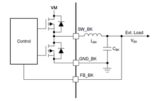
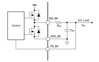
Figure 1 - Buck regulator in Inductor Mode (left) and Resistor Mode (right)
Overview
The buck regulator is a step-down mixed-mode regulator with configurable output voltages (3.3V, 4.0V, 5.0V, or 5.7V), low quiescent current (1-2mA), and protection circuits.
The following buck inductor and buck resistor values should be used for the following buck load currents:
- LBK = 47uH --> 0-200 mA load current
- LBK = 22uH --> 0-50 mA load current
- RBK = 22ohm --> 0-40 mA load current
There are also configurations for buck protections, power sequencing, and current limits that can be set to improve performance and robustness of the buck regulator.
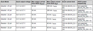
Figure 2 - Buck regulator configurations in the 8316 family
Efficiency
Buck regulator efficiency is a function of multiple parameters: VM, buck load current, and temperature. The following parameters will improve the efficiency of the buck regulator:
- Lower VM = better efficiency
- Higher load current = better efficiency
- Lower temperature = better efficiency
Inductor mode efficiency
With LBK = 47uH, the overall efficiency range is 57% to 95%. The highest efficiencies (74% to 95%) occur when VM <12V and the buck load current is near 200mA load current across all temperatures.
With LBK = 22uH, the overall efficiency range is 40% to 90%. The highest efficiencies (60% to 90%) occur when VM <12V and the buck load current is near 50mA load current across all temperatures.
Depending on the efficiency of the buck regulator, the total buck power dissipation can be calculated through the following equation:
P_BK = (1-η) * V_BK * I_BK (assuming η = buck efficiency)
For instance, if the DRV8316 is 5.0V, uses 180-mA, VM is 12-V, and a 47uH inductor for LBK is used, then the buck can be assumed to be operating near 90% efficiency.
The approximate buck power dissipation is:
P_BK = (1 - 0.9) * 5.0 * 0.18
P_BK = 0.09 W
Resistor mode efficiency
Resistor mode efficiency is negligible because power is dissipated through the external resistor rather than the buck, so device power losses and the junction temperature of the IC will decrease. Ensure the buck resistor is rated for the appropriate power by using the following equation:
P_RBK > (VM - V_BK) * I_BK
For instance, if VM = 24V and VBK = 3.3V with 30mA load current, then:
P_RBK > (24 - 3.3)*0.03
P_RBK > 0.621 W
A 3/4-W or 1-W rated resistor should be used for RBK.
Schematic / layout practices
Schematic practices
No matter if the buck is used or unused, the buck components RBK/LBK and CBK must be populated or else a buck undervoltage (BUCK_UV) fault is reported and the nFAULT pin goes low. If using a hardware variant of the device, the buck regulator cannot be disabled, so it recommended to use a small 22-ohm RBK resistor and 22uF capacitor to reduce the BOM of the unused buck.
BK_GND can be connected to AGND if noise coupling from PGND is mitigated. For best performance, use a separate ground for BK_GND and connect to AGND using a low-inductance component, i.e. net tie or wide 0-ohm resistor. For instance, the DRV8316REVM connects BK_GND to AGND because there is noise separation between AGND and PGND.
Layout practices
For best performance, separate SW_BUCK and FB_BUCK nets with ground separation. For instance, 25 mil separation of grounding is used in the DRV8316REVM between the SW_BK and FB_BK nets. This reduces coupling from the SW_BK into the buck output voltage FB_BK. It is also recommended to make SW_BK and FB_BK as wide as possible to allow for faster load switching.
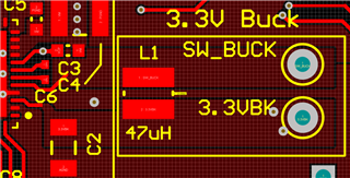
Figure 3 - Buck layout example on the DRV8316REVM
Troubleshooting
|
Issue |
Workaround |
|
BK_FLT bit is asserted or nFAULT is low upon device powerup |
Check if buck components are connected correctly and FB_BK > VBK_UV. |
|
SW_BK has 2.2MHz ringing |
Appears on DRV8316, DRV8316-Q1, MCT8316Z, MCT8316Z-Q1, MCF8316A, and MCT8316A devices due to discontinuous mode operation. External RC snubber between SW_BUCK and GND_BUCK can reduce ringing but cause a drop in buck efficiency. Use grounding separation between SW_BK and FB_BK so ringing does not couple into the buck voltage. |
|
Buck output voltage is not correct |
Ensure the BUCK_SEL bits are set to the correct setting (SPI/I2C devices), or the VSEL_BK pin has the correct resistor value set (Hardware devices) |
|
Buck output ripple is large |
There is too much resistance or not enough capacitance in CBK bypass path. Ensure the layout has low impedance, the CBK capacitor has a low ESR rating, and CBK is a VBK-rated to avoid capacitance derating. |
