This thread has been locked.

If you have a related question, please click the "Ask a related question" button in the top right corner. The newly created question will be automatically linked to this question.

DRV8432: output pulse issue

Part Number: DRV8432

Hi team,

Here's an issue from the customer may need your help:

Output a pulse signal of less than 1us at PWM frequency, as shown in the following figure:

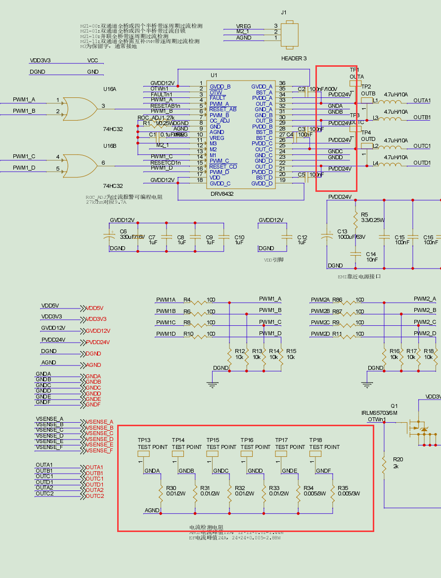
And the schematic is as follows:

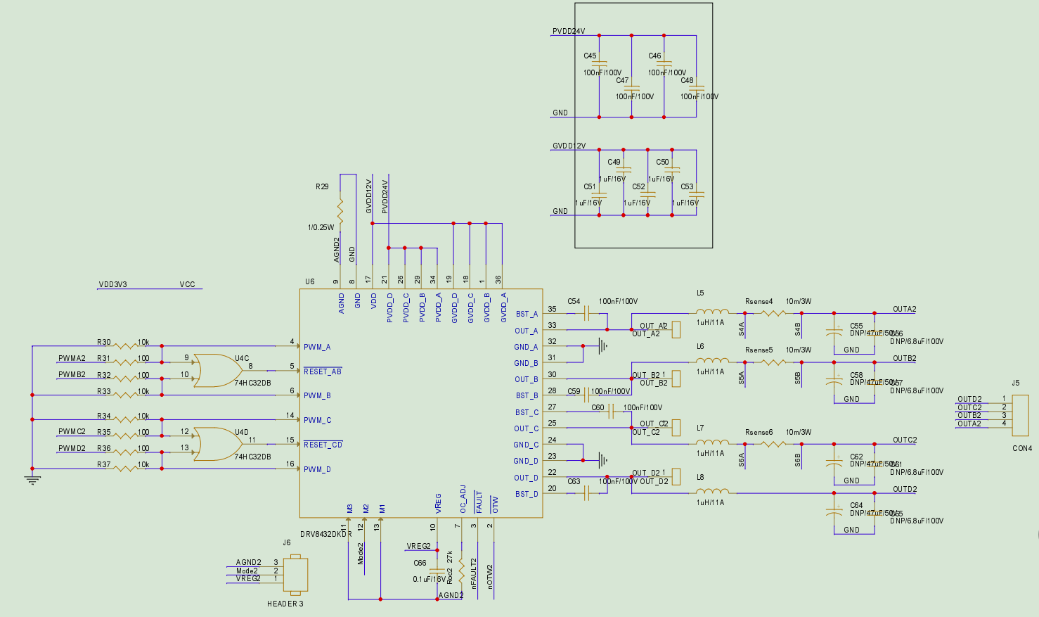
The input and output of the 74HC32 are as follows, the point is the time to generate the dead band. The DRV8432 supply pins have been tested and no problem.

Could you help check this case? Thanks.

Best Regards,

Cherry

  • Hi Cherry,

    Can you clarify what the problem is? Sorry, I was able to follow what the problem is. Is it the output signal not following the input signal?

    Regards,

    Pablo armet

  • Hi Pablo armet,

    Thanks for your support first!

    Please let me clarify, the input is a square wave with a frequency of 10 kHz and a duty cycle of 50% while the output is a pulse of less than 1 us. The previously painted board is normal, but once the current-sense resistor is placed from the low end to the high end, the new board drawn from GND_A-F ground is not working.

    Thanks and regards,

    Cherry

  • Hi Cherry,

    but once the current-sense resistor is placed from the low end to the high end, the new board drawn from GND_A-F ground is not working.

    Sorry once again. Can you clarify what you mean?

  • Hi Pablo,


    The figure above shows the schematic from the previous release, moving the highlighted current-sense resistor to the high-end detection on OUT_X, following the datasheet and evaluation board schematic of the DRV8432, with no changes to the rest. Now this latest version with pulse output issue and the previous one was working properly.

    If you need any other info please let me know.

    Thanks and regards,

    Cherry

  • Hi Cherry,

    Thanks for the explanation.

    I'm still not fully understanding the issue but I have a better idea now. Basically in their old design, they had the sense resistor connected between the GND of each bridge and PCB GND (GNDx/AGND). And in the new one, the placed the sense resistor in High-side sensing configurations. Resistor is placed between main power supply and GVDDx pins. Is this correct?

    Also, the issue with the output voltage only happens with the new design and not the old. Can you clarify if my understanding is correct?

  • Hi Pablo,

    The sense resistor in the new design is not connected between GVDD and PVDD, but between OUTx (Rsense4-6) The old design is working.

    But the old design did not split the digital and power lands. The new design is digitally separated from the power supply ground by magnetic beads, while the old design of the pin9 AGND of the DRV8432 is connected to the analogue ground, and the new design only has a path to the 1Ohm resistor of the pin8 GND.

    Thanks and regards,

    Cherry

  • Cherry,

    Understood. Have they measure the voltage potential between he two GNDs? If the GNDs have very different potentials, this could lead to logic problems in the IC.

  • Hi Pablo,

    We found the case here, after removing the DNP capacitors at the C55 outputs, all is good. Why is that? 

    Thanks and regards,

    Cherry

  • Hi Cherry,

    Great news. I think the 47uF caps is causing very large inrush currents during start-up causing the driver to go into current limiting mode. There is a minimum ON time so the small spikes are probably that.

    What load are they driving? is it a motor or solenoid?

    Regards,

    Pablo Armet

  • Hi Pablo Armet,

    What load are they driving? is it a motor or solenoid?

    The case here is they are without any load. Thanks for your support!

    Best Regards,

    Cherry