This thread has been locked.

If you have a related question, please click the "Ask a related question" button in the top right corner. The newly created question will be automatically linked to this question.

TMS320F28069M: Custom Board Design failing Instaspin Lab 01c

Part Number: DRV8301
Other Parts Discussed in Thread: TMS320F28069M, , , , STRIKE, CSD88599Q5DC

Hello,

This is related to the thread

https://e2e.ti.com/support/microcontrollers/c2000-microcontrollers-group/c2000/f/c2000-microcontrollers-forum/1061461/tms320f28069m-custom-board-design-failing-lab-01c/3953823?tisearch=e2e-sitesearch&keymatch=%25252525252525252520user%2525252525252525253A294039#3953823

entitled "TMS320F28069M: Custom Board Design failing Lab 01c." I was working with Aaron Barrera at the time, so he's the most familiar with it.

Anyway, I made the changes requested, and ran the final design past Aaron. Then I got caught up in the communications aspect of this project for a couple months.

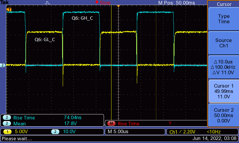
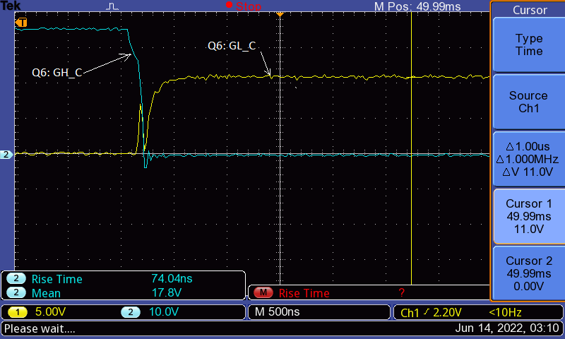
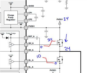
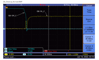
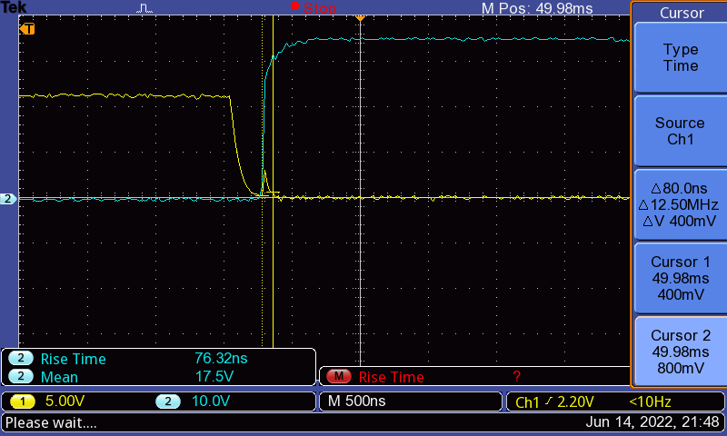
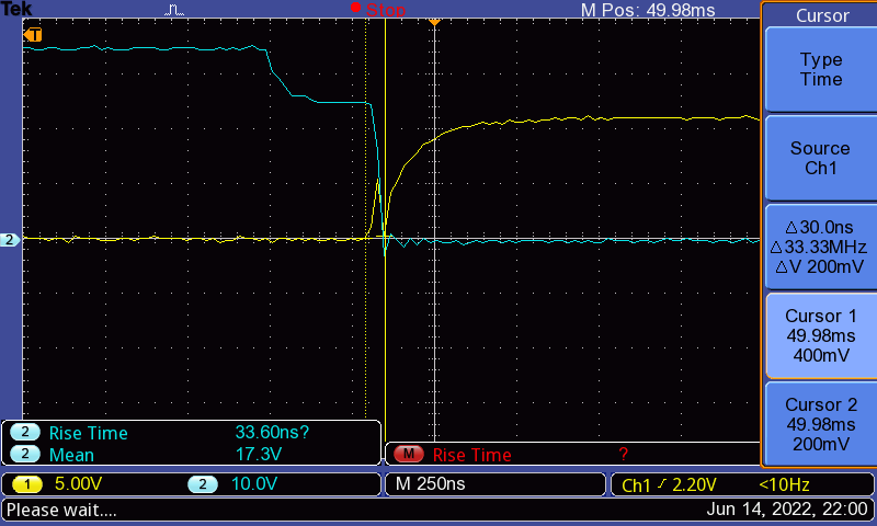
I just recently tried running the InstaSpin Labs again, and as soon as I set Flag Enable System and Flag Run Identify to 1, Q6 on my board starts spitting out smoke (it's only Q6 that's getting damaged).

The functional relationship between all parts is the same as the previous version, where I could at least get the motor to respond somewhat, without burning anything up.

The only changes were to the pcb layout - I'm now using polygon pours to widen the high current traces.

It almost seems like the gates of the 2 FETs in Q6 must be tied together, allowing 3v to be connected (nearly) to ground, but I already checked for that and ruled it out.

The other possibility that springs to mind is that somehow the firmware is turning on both FETs simultaneously, but this firmware works on the Evaluation Board (DRV8301-69M-KIT).

Thanks,

Dave

  • Sorry - I meant to say "allowing 24v to be connected (nearly) to ground."

    Just tried connecting three 18 ohm, 10W resistors in a "Y" configuration, to simulate a motor, but with a much higher resistance (hopefully limiting the current). I could see some pwm-like activity at the "motor" terminals, but only for a couple of seconds - then the waveform disappeared. I could smell smoke, so I removed power. Both FETs in the dual FET package Q6 look like a dead short from Drain to Source now (did not look that way before trying to drive the simulated motor). So just reapplying power results in more smoke. The other two FET pairs look ok.

    Thanks,

    Dave

  • Hi Dave,

    I dealt with a similar experience earlier this year on BOOSTXL-DRV8301 with LAUNCXH-F28069M, where there may be overcurrent events happening after a few PWM periods but then a fault triggers. 

    As a reminder, can you share with me:

    - Gate current setting used in SPI
    - Gate resistor values used

    Can you confirm if your GHx/GLx waveforms are having a shoot through event like below? 

    One thing we found in some code is that with InstaSPIN-FOC is that the BOOSTXL-DRV8301 does not turn on the LS FETs first every time the 50% PWM initialization sequence is started. With DRV8301 being a bootstrap based device, the expectation is to turn on LS FETs to charge bootstrap cap first and supply current to HS FETs. The algorithm intermittently turns on the HS FETs first, and when those are turned on first, you may experience a false OC events due to VDS marginally exceeding OC_ADJ_SET threshold value (~400ns after INHx = high, deglitch time is 400-500ns).

    Does the event above seem pertinent to your situation?

    Thanks,
    Aaron

  • Hi Aaron,

    The gate current is set to 0.25A - the lowest value available.

    The gate resistor values are 1 ohm. That might be the problem. I think we found that raising that value to 27 ohms made the rise of the gate voltage a little gentler, but didn't improve the behavior overall. The motor was still just jerking & shuddering.

    I have 15 boards and I've already killed Q6 on 3 of them. I don't know if I want to risk a couple more just yet, since neither the original FET that I specified nor the replacement part that I settled for are in stock anywhere right now.

    I guess I thought that the only problem was the skinny traces, and that the polygon pours would fix everything - silly me.

    I'll try 27 ohm for those base resistors, and risk burning up another FET, if you think it's a good idea, though.

    The original FET specified is the BSO150N03MDG. The replacement FET is the STS8DNF3LL. Specs are similar:

    Ciss for the BSO150N03MDG is 970pF. Ciss for the STS8DNF3LL is 800pF.

    Qg for the BSO150N03MDG is 12.6nC. Qg for the STS8DNF3LL is 12.5nC.

    Here are links to the data sheets:

    STS8DNF3LL

    BSO150N03MDG

    Thanks,

    Dave

  • Hi Aaron,

    When you said " the expectation is to turn on LS FETs to charge bootstrap cap first," did you mean the caps that are in parallel with the current sense resistors? If so, how could they get charged without the circuit being completed? Doesn't the high side FET need to be On in order for energy to be transferred through 2 coils to the RC network on the Low side? Or if there was some current circulating from the previous round, does just turning one transistor On cause some inductive kickback to charge the cap?

    Should I have larger capacitor values for the caps in parallel with the sense resistors? They're 0.001uF right now.

    If the timing for turning HS FETs On is less than the deglitch time, should I be adding dead time?

    If the OC you refer to above stands for OverCurrrent, the I assure you it's not a "false OC event." It's burned up a few FETs already.

    Thanks,

    Dave

  • Hi Dave,

    I am reading through your info and am leaving a detailed reply by end of the day today. 

    Thanks,
    Aaron

  • Ok - thanks Aaron!

  • Hi Dave,

    A few things in regards to your last replies. 

    The original FET specified is the BSO150N03MDG. The replacement FET is the STS8DNF3LL. Specs are similar:

    Ciss for the BSO150N03MDG is 970pF. Ciss for the STS8DNF3LL is 800pF.

    Qg for the BSO150N03MDG is 12.6nC. Qg for the STS8DNF3LL is 12.5nC.

    1) The MOSFET Qgd values you shared are very small, so increasing the gate resistance can help. I do not know how the gate current is when 27 ohms is introduced, but considering the Qgd of the MOSFETs are 4.5nC and 1.4nC respectively, this means the gate current shouldn't be more than 14mA worst case (1.4ns/100ns) to slew the VDS MOSFET voltage faster than 100ns. Increasing the gate current may help more if you know that a shoot through condition is not happening causing the short condition. 

    2) To confirm how the overcurrent condition is occurring, can you confirm using an oscilloscope whether:

    • The VGS voltage of the high-side MOSFET (GH_x-SH_x) and the low-side MOSFET (GL_x-SL_x) is on at the same time (VGS higher than the FET threshold voltage)? I do notice the Vgs(th) values for both these FETs are very low (~1-2V), so if the gate drive current is too low, then there is likely shoot through current occurring. Adding additional MCU dead time at the inputs or increasing the resistance at the DTC pin will be helpful. 

    • When the gate drive current is too high and you're switching a large amount of current through the MOSFET, it is possible that the motor voltage can couple into the low side gate voltage. Since the Vgs(th) values for these FETs is small, any spike on the low-side VGS voltage can cause the same type of shoot through condition to occur and cause damage to the MOSFET.

    When you said " the expectation is to turn on LS FETs to charge bootstrap cap first," did you mean the caps that are in parallel with the current sense resistors? If so, how could they get charged without the circuit being completed? Doesn't the high side FET need to be On in order for energy to be transferred through 2 coils to the RC network on the Low side? Or if there was some current circulating from the previous round, does just turning one transistor On cause some inductive kickback to charge the cap?

    3) To charge the bootstrap caps (red circle below), the low-side MOSFETs should be turned on first (blue circle below) in order to charge the bootstrap caps to GVDD so that when the high side FETs are turned on, there is sufficient gate drive current. If the high side FETs attempt to be turned on first without the bootstrap caps charged, there will not be sufficient gate drive current to support high duty cycles. 

    Should I have larger capacitor values for the caps in parallel with the sense resistors? They're 0.001uF right now.

    4) I do not think these caps are affecting performance. They can be used to smoothen the edges of the shunt voltages if there is high frequency transients from shunt inductance.

    If the timing for turning HS FETs On is less than the deglitch time, should I be adding dead time?

    5) Dead time would be good for the first bullet in item #2, either from the MCU or the DTC pin. 

    Thanks,
    Aaron

  • Hi Aaron,

    Thanks for the information and advice. I, of course, have some additional questions, numbered as your replies were above:

    1. So, to test this, I may have to sacrifice a few more FETs?

    2. Is there a calculation that will put me in the ballpark for just how much dead-time I might need? If not, would it be wise to crank it all the way up to 500nS, or right in the middle at 250nS? Or should I creep up slowly?

    I assumed the gate drive voltage would be 0-3.3V. It's more like 10V, so realistically Vgs(th) should be around 5V.

    so if the gate drive current is too low, then there is likely shoot through current occurring

    I thought the problem was that the gate drive current is too high?

    The first figure you attached has a resistive/ capacitive load. Would it be advisable to use this as a test circuit for my board?

    Could I avoid blowing up FETs (or burning up motors) this way. I already tried using 22 ohm as a load (3 of them in a "Y" configuration), but I still smoked Q6. Still, the resistances in the ckt you presented are much higher.

    3. I think you may have forgotten to attach a figure. I don't see anything with a "blue circle" or a "red circle."

    4. Ok thanks. I think I was just confused as to what you were calling the "bootstrap caps." I looked it up, and I think I understand how this works. In order to charge the bootstrap caps, one end of the cap must be connected to common, so that means the low side FET must be on first.

    So, the upshot of all this appears to be that I've selected the wrong MOSFETs. I need something with a considerably higher Ciss, Qgd, Vgs(th), and rise-time (which would be higher anyway if Ciss & Qgd are higher). A lower Rds(on) would probably be helpful, too, in order to lower the power dissipated by the FET when it's On.

    What I should have done from the beginning was to try and emulate the SUM110N06, used in the evaluation module, as closely as possible. Of course, I don't need anything with such high max currents or voltages. But all other parameters should mimic that device as much as possible. It'd be great if I could find something in the same package as I'm currently using, but I fear that's probably not possible, especially given today's supply chain issues.

    I'll make whatever changes I need for the next spin, but concurrently, though, I'll try and get the board up and running, with what I have. Do you really think it's doable? Will I just be endlessly chasing all these parameters around (dead time, gate resistance, dividing Vgs down, testing with dummy loads) while every change affects the others, so that finally I'm swept into some black hole of interdependence, when I could have just changed the FETs to something reasonable?

    Thanks,

    Dave

  • Hi Aaron,

    Well I'll be dipped. I had already changed the gate resistors to 27 ohms. I was just going to change them from 1 ohm (so I thought) to 27, when I saw that they were already there. So that must not be the problem, unless they need to be raised even higher. I had evidently changed the BOM, and then forgot about it.

    Dave

  • Hi Aaron,

    I've attached scope captures of GL and GH on Q6. The names of the files speak for themselves. In the closeup, it's pretty obvious that both gates are being turned On, at least partially, at the same time. These captures were obtained in the first 5 seconds or so after activating the firmware (Flag_Run_Identify & Flag_Enable_Sys both High). I played around with one board a little too long, and burned another FET (there's also a little square burn mark on my left index finger), so I suspect that the simultaneous on-time gets worse as time progresses. A couple of thigs that strike me as odd:

    GH has a much higher amplitude than GL, and

    Removing Q6 doesn't result in some other FET pair getting smoked.

    GH_C & GL_C - Q6 Removed - No Load.BMP

    Q6_No-Load.BMP

    Q6_Close-up_No load.BMP

    Best Regards,

    Dave

  • Hi Aaron,

    Looks like GL & GH need to be moved apart by approximately 200ns, so I'll set the DTC to 250ns, with a 75k ohm resistor (or as close as I can get). Does this seem like a good plan?

    Thanks,

    Dave

  • Hi Dave, 

    I'm reading through all your info now, give me a few minutes and I'll have feedback.

    Thanks,
    Aaron

  • Hi Dave,

    Thanks for the information and advice. I, of course, have some additional questions, numbered as your replies were above:

    1. So, to test this, I may have to sacrifice a few more FETs?

    2. Is there a calculation that will put me in the ballpark for just how much dead-time I might need? If not, would it be wise to crank it all the way up to 500nS, or right in the middle at 250nS? Or should I creep up slowly?

    I assumed the gate drive voltage would be 0-3.3V. It's more like 10V, so realistically Vgs(th) should be around 5V.

    Our DRV83x gate driver devices supply around 10V for enhancing N-type power MOSFETs. We recommend MOSFETs with higher threshold voltages around 4V, typically these FET datasheets have specified Rds(on) values for VGS = 4.5V or 10V. But we do not recommend logic-level FETs for these reasons. 

    When choosing a FET, the expectation is that FETs should only be sacrificed if problematic FET switching issues occur, such as a shoot-through current because both FETs are on, a FET gets stuck on/off, or large coupling event from the motor voltage into a FET's gate voltage. The DRV8301's internal protections will try and prevent these issues from occurring by monitoring VDS overvoltage, inserting programmable dead time, etc. 

    Let's analyze dead time more in a bit. 

    GH has a much higher amplitude than GL, and

    This is because when you turn on GH_x, it needs to be 10-V than the motor voltage which is at the high-side source pin (SH_x), so our DRV8301 part turns on GH_x to be SH_x + 10V, hence your supply voltage is 24V to GH_x with respect to GND turns on to 34V so that the high-side Vgs (gate-to-source voltage) is 10V. 

    See below when you switch the GH_A on, the gate driver turns on GH_A so that it increases to 34V while SH_A increases to 24V to the Vgs of the HS FET's gate increases to 10V. 

    Now let's look closely how the FETs are turning on to see if they're turning on at the same time. 

    With no load, we see that GL_C is turning on at GH_C is turning off. It's hard to tell looking at just GH_C itself whether the high-side FET is actually on because we need to look at GH_C - SH_C (gate to source voltage) to see if Vgs < Vth, but knowing PVDD=24V and the low Vth of the FETs, it is very likely that these are turning on at the same time every PWM cycle, which will result in a lot of current flowing through the FET and excessive heating. 

    To resolve this, I would add at least 250ns of dead time as you mentioned. You can do this either by adding the 250ns at the MCU inputs (INH_x/INL_x), or by increasing the DTC resistor to a value that corresponds to 250ns, so the 75kohm resistor should be fine. 

    Thanks,
    Aaron

  • Hi Aaron,

    Given what's happening, I'd say they're almost certainly turning On at the same time.

    I tried a 68k resistor at DTC, and saw the following at the FET gates (Blue is GH_C, and yellow is GL_C):

    Looks like the duration of the overlap of the extra GL_C pulse and the GH_C was decreased from 200ns to 80 ns, and the amplitude of that extra pulse is smaller (probably just this one instance - I think I saw others that were higher than the one pictured here).

    I didn't like the looks of it, though, at the time, and was hoping to completely eliminate any overlap, so I increased the DTC resistor to 120k, which resulted in an overlap of only 30ns, as shown below:

    The amplitude looks like enough to activate the gate, but it's for a much shorter period.

    Unless you have any other suggestions, I'm going to try and let this run for an extended period, and see whether it blows the FET again.

    If it works, that's great - we can at least do some testing with these boards.

    In any case, I plan on selecting a replacement for the FETs. I've narrowed it down to 2:

    FDI038AN06A0

    OR

    CSD88599Q5DC

    I think I prefer the CSD88..., even though the specs aren't quite as good. The FDI038... is through-hole and would take up a lot more real estate on the PCB.

    Let me know what you think, regarding whether either one of them will work, without a whole lot of fussing around.

    Thanks,

    Dave

  • Hi Aaron,

    This is fantastic! It's almost miraculous. I've been running the Instaspin firmware on the board (no load), for about 10 minutes now, and Q6 isn't even getting warm. Usually, it would start smoking in less than a minute.

    Are there any undesirable side effects of adding so much dead-time? I know crossover distortion can be an issue with audio circuits if one transistor in a push-pull amp turns turns on much later than the other turns off - could there be a similar effect here?

    Is there anything I should watch out for once I connect the motor?

    Thanks,

    Dave

  • Hi Dave,

    Glad to hear that dead time is working! That's the benefit of dead time, as soon as those gate signals turn on at the same time bad things happen due to the large amount of current shooting through the FETs from supply to ground. 

    The biggest disadvantage I am aware of is that in a motor drive application, more dead time results in less drive overhead for a motor load. It will not be able to supply as much motor current because there will be less FET conduction time at higher duty cycles since the DRV8301 prioritizes dead time over the gate drive waveforms. 

    For instance, if you are using 50us PWM period (20kHz), and you need 500ns dead time, then this will occur twice in a PWM period during the MOSFET switching events (beginning and end), so then the max duty cycle you'll be able to drive is 98% duty cycle (49us) because the DRV8301 will prioritize the 2*500ns of dead time to prevent shoot through events. 

    Thanks,
    Aaron

  • Hi Aaron,

    Well... that's not the greatest news. We're using a relatively low inductance motor, which necessitates using a 45 kHz PWM.

    So I'm definitely doing another spin with a different FET.

    But this is a nice fix for the prototype phase.

    Here are some of the salient CSD88599Q5DC specs (worst ones first):

    Vgs(th) = 2.5V

    Qgd = 7nC

    tr = 20ns

    Ciss = 3.72nF

    Rds(on) = 2.5mohm

    Id = 40A

    Pkg Dim = 5mm x 5mm

    Likewise for the FDI038AN06A0:

    Pkg = TO-220

    Id = 17A

    Rds(on) = 3.8 mohm

    Vgs(th) = 3V

    Ciss = 6.4nF

    Qgd = 27nC

    tr = 144 ns

    Do these look ok?

    Thanks,

    Dave

  • Hi Dave,

    For MOSFET selection, I would advise in this case to pick a MOSFET with a higher Vgs(th) value so that you can avoid the other FET turning on while a FET is turning off. The higher the Vgs(th) value, the less likely this shoot through condition is to occur because of the low Vgs(th).

    If you are looking to avoid changing the BOM, then picking a FET with similar Qgd values will have similar gate turn on/off behavior to what you are seeing now. The higher the Qgd, the slower the Vgs turn on/off will be because it will take a longer time to slew the VDS voltage, which can help with reducing this dV/dt coupling behavior you are seeing before (where the LS FET turns on prematurely due to motor voltage coupling into the LS gate)

    I would prefer the FDI038AN06A0's specs, but the TO-220 package is not preferred because of the inductance of the leads on the package. So CSD88599Q5DC would be a better candidate for this. 

    Thanks,
    Aaron

  • Thanks Aaron! I'll keep looking for something in an appropriate package, with higher Vgs(th) and higher Qgd - these were just the best I've encountered so far.

    I'm marking his resolved.

    I see you were a music minor. I know this forum isn't for small-talk, but what instrument(s) and what kind of music? I'm a guitar player myself, most recently in a bluegrass band in Delaware called Chapel Street Junction; haven't been playing much lately, though.

    Thanks again,

    Dave