This thread has been locked.

If you have a related question, please click the "Ask a related question" button in the top right corner. The newly created question will be automatically linked to this question.

DRV8841: Connecting two outputs together

Genius 17405 points
Part Number: DRV8841

Hi Experts,

Good day. Seeking your assistance on this query:

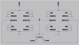
I would like to use the DRV8841 to drive a stepper motor. The issue is that this motor has a particular wiring and two phases, like shown in one of the attached pictures.

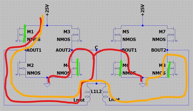
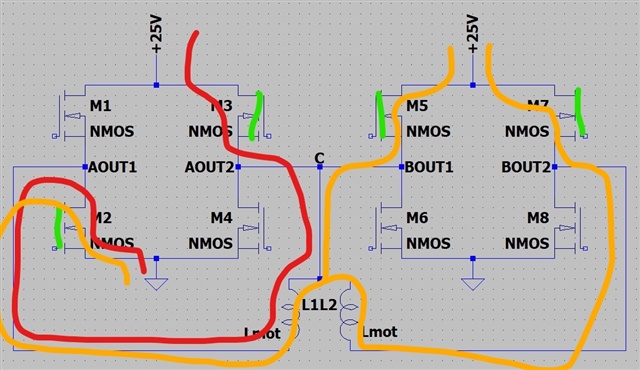
I would like to ask you if I can plug the common wire of the motor (C) to the H_bridges like it is shown in the example schematic I attached.

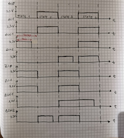
If the motor is excited like the excitation method that is shown, is there any risk that some short circuit can occur, or that the other phase may be energized when it shouldn't be?

Besides, when I set, for example, both the pins AI0 and AI1 to 0 (which corresponds to no current flow through the A H-bridge), the datasheet states that in this case that H-bridge is disabled. Does this mean that the outputs are in a high impedance state? So, if yes, no current can flow from the common point (C) to AOUT2 and then to ground through the low-side MOSFET (M4 in the picture)?

Thank you.

Regards,
Archie A.


  • Hi Archie,

    The main issue I see with this configuration is potential 25V to GND short on AOUT2 and BOUT1. Both H-bridges not not fully sunchronized since each bridge is control by different control signals (AINx, BINx).

    Can you provide the control sequence you plan to use.

    Regards,

    Pablo Armet

  • Hello Pablo,

    Thank you for your response.

    I am attaching the control sequence I plan to use and some pictures describing the situations I expect in each state of motor coil excitement. Here are some info about the control that might help you:

    - Each phase of the motor has a maximum resistance value of 343 Ohm and a maximum inductance value of 225 mH;
    - 6 ms < Tstep < 600 ms;
    - Duty cycle (Ton/Tsetp): between 95% and 100%.

    Regarding the pictures I attached, together with the observation of the excitation sequence, I have some doubts, that will be written in the following message, seeing that there is a limit of characters that can be used.

    In every one of them, the green lines represent the expected activated MOS, the red lines represent the expected (and desired) current path for that state and the light orange lines represent an exptected (and not desired) current path for that state.
    - For "state 1" pic: is it possible that the bridge A can excite the right winding through the orange current path? Even though, as you can see from the excitation sequence, I set BI0 and BI1 to 1 so that no current can flow through the bridge B (a similar issue occurs for state 2)?
    - For "state 3" pic: are any, or both, of the two orange current paths possible? Even though, through pins BI0 and BI1 I set a 0 current for bridge B (a similar issue occurs for state 4)?

    Regards,
    Archie A.

  • Hi Archie,

    Thank you for the detail sequence description.

    Firstable, let me answer one of the questions you asked in the first post:

    Besides, when I set, for example, both the pins AI0 and AI1 to 0 (which corresponds to no current flow through the A H-bridge), the datasheet states that in this case that H-bridge is disabled. Does this mean that the outputs are in a high impedance state?

    This is correct, typically when we say bridge disabled, it means the h-bridge FETs are high-z.

    For "state 1" pic: is it possible that the bridge A can excite the right winding through the orange current path? Even though, as you can see from the excitation sequence, I set BI0 and BI1 to 1 so that no current can flow through the bridge B (a similar issue occurs for state 2)?

    Since BIx is set to 0, the H-bridge will be High-Z . Therefore, not current should flow through H-bridge B.

    - For "state 3" pic: are any, or both, of the two orange current paths possible? Even though, through pins BI0 and BI1 I set a 0 current for bridge B (a similar issue occurs for state 4)?

    I'm a bit confused as to why you have BIN1 and BIN2 = 1 in state 3 when you set BI0 and BI1 to 0. The H-bridge B FETs will be high-Z in this case regardless of the BINx. So no concern with current flowing in the orange path.

    Regards,

    Pablo Armet