A related question is a question created from another question. When the related question is created, it will be automatically linked to the original question.
If you have a related question, please click the "Ask a related question" button in the top right corner. The newly created question will be automatically linked to this question.
Got it...thank you for the additional explanation.
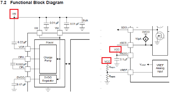
There are no timing requirements necessarily between VM and VCC.
However, VCC definitely should be stable before any SPI communication as this is the reference for the SDO output buffer. Also, VCC should be stable before issuing any pulses on the STEP input as VCC is the reference for current regulation in the device.
And of course VM should be up before communication or stepping as VM is the source for all the internal regulators.
VM can be up first without VCC. There is no reliability concerns for VM applied to the device BEFORE VCC. This is OK.