This thread has been locked.

If you have a related question, please click the "Ask a related question" button in the top right corner. The newly created question will be automatically linked to this question.

DRV8412: Peak current protection issue

Part Number: DRV8412

Hi team,

Here's an issue from the customer may need your help:

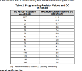
The device has its own peak current protection, which is latched above the peak current, and must be reset before it can be released.

1) The customer would like to know if the peak overcurrent protection (OC)  can be removed, since the manual simply states that the resistor can be adjusted to change the amount of peak current.

2) how long does the current last to trigger peak current protection, 10ms?

3) when reset, the reset pin needs to be pulled low and then pulled high. At least how long does the low level last? 

Could you help check this case? Thanks.

Best Regards,

Cherry

  • Hi Cherry, 

    Absolutely. Allow me to look over the details of the datasheet and expect a response in the next 24 hours. 

    Best,

    Pedro Arango Ramirez

  • Hi Cherry,

    1. An OC_adj resistor is needed in order to protect the device from higher currents than it can withstand. please refer to the following table: 

    2. The overcurrent response time can be found in the electrical characteristics of the datasheet; 250ns: 

    3. Seeing how the PWM frequency is 500kHz it is safe to assume that the reset pin will also be able to catch the rising and falling edge in this time. The following section has more information about it: 

    7.3.3 Device Reset Two reset pins are provided for independent control of half-bridges A/B and C/D. When RESET_AB is asserted low, all four power-stage FETs in half-bridges A and B are forced into a high-impedance (Hi-Z) state. Likewise, asserting RESET_CD low forces all four power-stage FETs in half-bridges C and D into a high- impedance state. To accommodate bootstrap charging prior to switching start, asserting the reset inputs low enables weak pulldown of the half-bridge outputs. A rising-edge transition on reset input allows the device to resume operation after a shut-down fault. For example, when either or both half-bridge A and B have OC shutdown, a low to high transition of RESET_AB pin will clear the fault and FAULT pin; when either or both half-bridge C and D have OC shutdown, a low to high transition of RESET_CD pin will clear the fault and FAULT pin as well. When an OTSD occurs, both RESET_AB and RESET_CD need to have a low to high transition to clear the fault and FAULT signal.

    Best,

    Pedro Arango Ramirez