This thread has been locked.

If you have a related question, please click the "Ask a related question" button in the top right corner. The newly created question will be automatically linked to this question.

UC3625DWTR has no output waveform

Hi team,

Here's an issue from the customer may need your help:

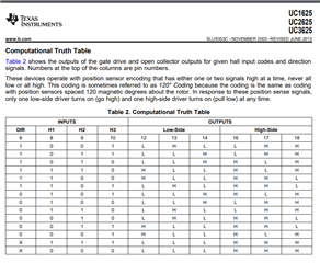
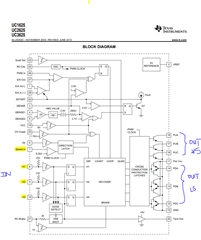
After several debugging, the PWR VCC+16V, VCC+16V supply pins are all +16V normal. When the RC-OSC pin is set to 2.0V-3.6V, the voltage of PDC pin, PDB pin, PDA pin are all 0V and cannot get the waveform from the oscilloscope.

The PBA, PUB and PUC pins all have voltages between 1.7V and 3.0V. But neither can the square waveform be detected. What could be the possible reason?

Could you help check this case? Thanks.

Best Regards,

Cherry

  • Hi Cherry,  

    Will look into this but may need some time since this is a very old device

    Targeting to give you an answer before end of next week 

    Best Regards, 
    Andrew

  • Hi Andrew,

    May I know is there any feedback on this?

    Thanks and regards,

    Cherry

  • Hi Cherry, 

    My apologies for the delay - I'll aim to get you a response before EoD tomorrow. 

    Best Regards, 
    Andrew 

  • Hi Cherry, 

    My apologies for the late response - 

    So looking at this device datasheet functionality, we see that the relationship of INPUTS (H1/H2/H3, DIR) on OUTPUTS (PUA/PUB/PUC, PDA/PDB/PDC) is shown by the table below. PUA/B/C is meant to drive high-side PMOS type FETs, and PDA/B/C is meant to drive low-side NMOS type FETs. 

    • The voltages you're describing suggest to me that the UCC device is not really able to drive the outputs ON at all currently. They seem to be remaining OFF. 

    Some questions to help debug: 

    1. is the customer seeing inputs toggle at H1/H2/H3? Any waveforms to share on this? If not, can they try to toggle them manually via GPIO or function-generator? 
    2. what is the signal inputted on 'SPEED-IN' pin? I am curious if the outputs are being disabled because the overcurrent protection is activating 

    Input-Output truth table

    ISENSE pin, which involves overcurrent protection & can trigger output shutdown

    Best Regards, 
    Andrew 

  • Hi Andrew,

    The voltage output from the regulated triode is normal and the IC is supplied with an 11-pin voltage of 18.4V and a 19-pin voltage of 16.6V.

    However, there is no voltage on pins 12-14, and pins 16-18, and no waveform output.

    Thanks and regards,

    Cherry

  • Hi Cherry, 

    Acknowledged that the device's outputs are not showing any activity according to your description,

    • but the outputs depend on the device inputs, not just being powered on at pin 19 (VCC) or pin 11 (PWR VCC) 

    Because of that, I am asking some questions in my earlier response to request that the customer help check other device inputs (such as H1, H2, H3, SPEED-IN) 

    Best Regards, 
    Andrew 

  • Hi Andrew,

    The customer has tried to debug as you said, but there's still no any wave had been output.

    Thanks and regards,

    Cherry

  • Hi Cherry, 

    In order for us to help debug further, we will definitely need waveforms and other system-level info I mentioned above.

    Can they help share more data (waveforms, voltage and current measurements) so that we can analyze it and find the problem? 

    Best Regards, 
    Andrew