


Other Parts Discussed in Thread: DRV8302, DRV8306, DRV8328, DRV8311, DRV8329, DRV832X, DRV8323, DRV8353
When using a Brushless-DC motor driver with a Hardware interface versus a SPI interface, there is a trade-off of having simpler device setting configurations but losing the ability to easily diagnose detected faults. On SPI devices, fault(s) will “latch” to specific bits in the status registers to easily diagnose the fault that occurred (such as VGS_HA indicating that a Gate Driver Fault occurred on the high-side MOSFET of phase A). But on hardware devices, the only indicator of a fault occurring is the nFAULT pin going low, which does help much when trying to diagnose a fault that occurred during evaluation.
In this E2E FAQ, we’re going to share some tips and tricks to help debug faults that occur when evaluating with Hardware devices by using known behaviors of Hardware devices.
BLDC Motor Drivers with Hardware Interfaces
Brushless-DC motor drivers with hardware interfaces are below. The devices in bold are commonly more difficult to debug due to the large amount of protection features in the device:
Gate drivers:
- DRV8302
- DRV8304H
- DRV8306
- DRV8320H/DRV8323H/DRV8320RH/DRV8323RH
- DRV8340H-Q1/DRV8343H-Q1
- DRV8350H/DRV8353H/DRV8350RH/DRV8353RH
Integrated MOSFET drivers:
- DRV8311H
- DRV8316T
- MCT8316Z0T
Hardware Device Behaviors
When a fault occurs, the protection mechanism for that fault has three parameters: a threshold, timing, and recovery mode. Additionally, some hardware devices with diagnostics automatically begin at powerup or operating mode.
The four main settings in a gate driver can have configurable thresholds, but the timings and recovery modes are defaulted for those protections to work. All of the other settings are defaulted to a threshold, timing, and recovery method.
The quickest way to determine the fault, condition, configuration, report, and recovery mode is to look at the Fault Action and Response table in the Gate Driver Protective Circuits section of the datasheet. From there, we can determine which faults will pull the nFAULT pin low and whether the fault will automatically recover, retry after a fixed timing, or remain in latched shutdown.
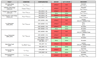
Figure 1 - Fault Action and Response table in DRV835x.
In summary, by knowing the timings and recovery methods of faults in relation to when the nFAULT pin goes low, we can deductively determine which fault(s) can occur and confirm by measuring the correct waveforms.
Common Hardware Faults and Diagnoses
The following are common types of faults in hardware devices, along with their timings and recovery methods.
Supply undervoltage (VM_UVLO, PVDD_UVLO)
Motor supply undervoltage lockout, which is typically VM or PVDD, occurs when the motor supply voltage is less than the falling undervoltage lockout threshold for longer than the undervoltage deglitch time. If this occurs, then the device will automatically shutoff, nFAULT will go low, and the logic will be disabled. Many times the fault will automatically recover if the motor supply voltage exceeded the rising undervoltage lockout threshold.
For example, in DRV8328, PVDD undervoltage occurs if PVDD is less than the falling undervoltage lockout threshold (VPVDD falling) for longer than tPVDD_UV_DG, and will recover when PVDD is above the rising undrvoltage lockout threshold (VPVDD rising).
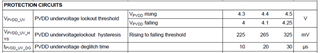
Figure 2 - PVDD undervoltage protection in DRV8328.
Generally, supply undervoltage this can occur from a few scenarios:
- Large current demands from the supply during motor startup, increased load conditions, or undetected shoot-through events
- Supply inductance causing transient spikes from the supply
- Insufficient supply bulk capacitance on the PCB
To measure if VM/PVDD undervoltage is occurring in waveforms, measure VM/PVDD and nFAULT. Use a falling trigger on nFAULT to see if the VM/PVDD is lower than the supply undervoltage threshold for longer than the device’s supply undervoltage deglitch time.
Charge pump undervoltage (CPUV)
Charge pump undervoltage lockout, which is typically VCP or CP, occurs when the charge pump voltage is less than the charge pump falling undervoltage lockout threshold for longer than the charge pump undervoltage deglitch time. If this occurs, then the device will automatically shutoff, nFAULT will go low, and the logic will be disabled. Many times the fault will automatically recover if the motor supply voltage exceeded the rising undervoltage lockout threshold.
For example, in DRV8311H, charge undervoltage occurs if CP is less than the falling undervoltage lockout threshold (VCP falling) for longer than tCPUV, and will recover when CP is above the rising undervoltage lockout threshold (VCP rising).
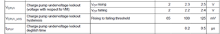
Figure 3 - Charge pump undervoltage protection in DRV8311.
Generally, charge pump undervoltage this can occur from a few scenarios:
- Charge pump storage capacitor (which is between the charge pump pin and driver supply pin) is placed far from the device, has too large of a current loop, is too small in capacitance, or has capacitance derating due to temperature or voltage bias
- Gate driver outputs are demanding more average gate drive current than the current capability of the device’s charge pump
- There is too much external load current on the charge pump if it is being used to drive an external load, such as a supply cutoff switch MOSFET
To measure if charge pump undervoltage is occurring in waveforms, measure VCP/CP, VM/PVDD, and nFAULT. Use a falling trigger on nFAULT to see if the charge pump voltage with respect to the supply voltage is lower than the charge pump undervoltage threshold for longer than the device’s charge pump undervoltage deglitch time.
Gate driver undervoltage (GVDD/VGLS)
Gate driver undervoltage lockout, which is typically GVDD or VGLS, occurs when the gate driver voltage is less than the gate falling undervoltage lockout threshold for longer than the gate driver undervoltage deglitch time. If this occurs, then the device will automatically shutoff, nFAULT will go low, and the logic will be disabled. Many times the fault will automatically recover if the motor supply voltage exceeded the rising undervoltage lockout threshold.
For example, in DRV8329, gate driver undervoltage occurs if GVDD is less than the falling undervoltage lockout threshold (VGVDD falling) for longer than tGVDD_UV, and will recover when GVDD is above the rising undrvoltage lockout threshold (VGVDD rising).
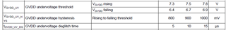
Figure 4 - Gate driver undervoltage protection in DRV8329.
Generally, gate driver undervoltage this can occur from a few scenarios:
- GVDD bypass capacitor (which is between the GVDD pin and driver supply pin) is placed far from the device, has too large of a current loop, is too small in capacitance, or has capacitance derating due to temperature or voltage bias
- Gate driver outputs are demanding more average gate drive current than the current capability of the device’s built-in GVDD regulator or external GVDD supplied
- There is too much external load current on the GVDD pin if it is being used to drive an external load, such as an external regulator or circuitry
To measure if GVDD undervoltage is occurring in waveforms, measure GVDD and nFAULT. Use a falling trigger on nFAULT to see if the charge pump voltage with respect to the supply voltage is lower than the GVDD undervoltage threshold for longer than the device’s GVDD undervoltage deglitch time.
Other undervoltage lockouts (Buck, DVDD, AVDD)
Although not as common as the previous supply undervoltage lockouts, the same strategies can be implemented to diagnose buck, DVDD, AVDD, or CSAREF undervoltage lockouts. If the supply is lower than its respective falling undervoltage lockout for longer than its deglitch time, then the nFAULT pin usually latches low until it is above its rising undervoltage lockout.
Some tips are below for various supplies in specific hardware devices:
- In DRV8316T, the nFAULT pin can go low at powerup due to a buck undervoltage lockout if the external buck components (LBK/RBK and CBK) are missing. They are required by design, even if the buck is unused.
- Generally, AVDD and DVDD undervoltage lockout can determine if logic inside the device is enabled or disabled since it is used to power logic. If an AVDD or DVDD undervoltage lockout occurs, logic is disabled and can result in re-latching hardware device pin settings.
VDS Overcurrent (VDS_OCP)
Overcurrent protection that is detected across each MOSFET’s drain-to-source voltage is active only when its associated INHx/INLx input is high. A VDS overcurrent event occurs if the VDS voltage exceeds the VVDS_OCP threshold voltage (which is set by the VDS or VDSLVL pin) for longer than the tOCP_DEG time. If this occurs, then on hardware devices the nFAULT pin will go low and shut off that MOSFET. Once nFAULT goes low, two things can occur:
- If the PWM input signal stays low, then the device will wait for tRETRY to automatically clear the fault and begin normal gate driver operation
- If the PWM input signal has a rising edge, the nFAULT will automatically clear and begin to operate the gate driver again if the device has cycle-by-cycle current limit automatically enabled (DRV832x/DRV834x/DRV835x only).
For example, in the DRV8350H, suppose the VDS pin has a 75kohm resistor tied to GND, which sets the VDS_OCP threshold voltage to 0.2V. The INHB pin goes high, so VDS will be actively monitored across VDRAIN-SHB while INHB is high.

Figure 5 - VDS pin settings in DRV832x hardware devices.
In this device, the tOCP_DEG time is 4 us by default. Suppose a short circuit event across the MOSFET occurs, causing a large voltage spike across the MOSFET. If the MOSFET’s VDS voltage is greater than 0.2V for longer than 4 us, then a VDS overvoltage has occurred and the nFAULT pin will go low while shutting off that gate driver.
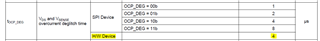
Figure 6 - VDS overcurrent deglitch time in DRV832x hardware devices.
Suppose that the firmware is setup to continue driving the PWM inputs at 20kHz frequency even though the fault has occurred. At the next INHB rising edge, which occurs every 50us, the nFAULT pin will automatically clear and try to drive the MOSFET gate again. This is called cycle-by-cycle current limit, which means the MOSFET will continue to shut off until the overcurrent condition is cleared during continuous operation.

Figure 7- Description of cycle-by-cycle current operation in DRV832x hardware devices.
Suppose that the firmware is setup to turn all PWM inputs off low after the nFAULT event is detected. The DRV8350H will wait 8 ms before releasing the nFAULT pin and trying to control the gate driver outputs again from the PWM inputs. This is called automatic retry, because the device will retry after the fixed retry time to return the system to a normal current before operating again. This is useful for fast, large overcurrent events, such as shoot-through currents or excessive voltage ringing across the VDS MOSFET.

Figure 8 - VDS overcurrent automatic retry time in DRV835x hardware devices.
Generally, VDS overvoltage can occur from a few scenarios:
- Too large of an IDRIVE setting causes fast VDS slew rates under 100ns. If the high-side MOSFET slews too fast, the switch node voltage can couple into the low-side MOSFET’s gate signal, which is referred to as dV/dt coupling or crosstalk. If the low-side MOSFET gate signal turns on, this can cause a shoot-through event through the half-bridge and trip VDS overcurrent protection. Selecting an appropriate IDRIVE setting, implementing RC snubbers, and having good powerstage layout can mitigate VDS overcurrent faults.
- Too low of an IDRIVE setting can cause slow VDS slew rates over 4ms. This can cause the MOSFET VDS voltage to above the VVDS_OCP value after tOCP_DEG, even though there is no real overcurrent event occurring. This is sometimes referred to as a “false overcurrent event”. Selecting an appropriate IDRIVE setting can mitigate false VDS overcurrent faults.
- Sometimes VDS overcurrent testing is tested purposefully by shorting the low-side MOSFET’s drain-to-source voltage while turning on the high-side MOSFET. This can cause the supply voltage to drastically dip while monitoring the high-side’s VDS voltage. It is not recommended to perform this testing as VDS monitoring can be affected when the supply and drain voltage is near its undervoltage lockout threshold. The preferred method to evaluate the VDS overcurrent protection of the DRV device is to remove the MOSFET and apply the VDS voltage across the drain-to-source monitoring pins that will trip overcurrent protection.
To measure if VDS overcurrent is happening in waveforms, measure nFAULT and trigger on the falling edge. If the nFAULT signal “clears” in the PWM period time (i.e. 10-50us), it is indicative of cycle-by-cycle overcurrent happening. If the nFAULT signal clears around after tRETRY, then it is indicative of automatic retry since the PWMs are being turned off when the overcurrent condition fault occurs.
To determine which FET the VDS overcurrent event is happening on, measure nFAULT, GHx, SHx, and GLx with single-ended probes (or GHx-SHx with a differential probe) to trigger on an nFAULT falling edge to see if each MOSFET’s VDS voltage is higher than the VVDS_OCP voltage after tOCP_DEG. You will need to zoom in close to around 1 us/div to analyze the VDS behavior for the high-side MOSFET (PVDD/VDRAIN-SHx) and the low-side MOSFET (SHx/DLx-SLx/SPx/LSS).
VSEN Overcurrent (SEN_OCP)
VSEN overcurrent (detected across each phase’s low-side shunt resistor) occurs if the differential voltage across the shunt resistor exceeds the VSEN_OCP or VSEN threshold voltage for longer than the tOCP_DEG time. On devices with three low-side current sense amplifiers (such as DRV8323/DRV8343/DRV8353), VSEN is active across SPx-SNx when its associated INLx input is high. If this occurs, then on hardware devices the nFAULT pin will go low and shut off that low-side MOSFET. Once nFAULT goes low, the device will wait for tRETRY to automatically clear the fault and begin normal gate driver operation.
For example, in the DRV8323H, the sense resistor overcurrent voltage (VSEN_OCP) is fixed to 1V. The INLC pin goes high, so the SPx-SNx voltage across phase C’s low-side shunt resistor will be actively monitored to detect if an overcurrent condition occurs.
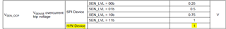
Figure 9 - VSEN_OCP default threshold in DRV832x hardware devices.
In this device, the tOCP¬_DEG time is 4 us by default. Suppose a short circuit event across the low-side MOSFET occurs, causing a large current spike through the shunt resistor while VDS protection is disabled. If the voltage across the shunt is greater than 1V for longer than 4 us, then a VSEN overvoltage has occurred and the nFAULT pin will go low while shutting off the phase C low-side MOSFET.
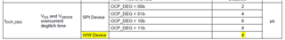
Figure 10 - VSEN_OCP overcurrent deglitch time in DRV832x hardware devices.
Suppose that the firmware is setup to turn all PWM inputs off low after the nFAULT event is detected. The DRV8323H will wait 4 ms before releasing the nFAULT pin and trying to control the gate driver outputs again from the PWM inputs. This is called automatic retry, because the device will retry after the fixed retry time to return the system to a normal current before operating again. This is useful for fast, large overcurrent events, such as shoot-through currents or excessive voltage ringing across the shunt resistor.

Figure 11 - VSEN_OCP automatic retry time in DRV832x hardware devices.
Generally, VSEN overvoltage can occur from a few scenarios:
- If VDS protection is disabled, dV/dt coupling (described in VDS overcurrent protection above) can cause a shoot-through event through the half-bridge and shunt resistor. Enabling VDS protection, selecting an appropriate IDRIVE setting, implementing RC snubbers, and having good powerstage layout can rule out the possibility of VSEN overcurrent faults.
- If the shunt resistor is too small, or if the motor current path from the low-side MOSFETs to the shunt resistor to the supply ground is insufficient, then added inductance can cause larger spikes near the shunt resistor’s SPx-SNx pins. If the voltage spikes exceed 1V for longer than the overcurrent deglitch time, this could falsely trip VSEN overcurrent protection. To prevent this from occurring, ensure there is sufficient layout for the motor return current path, the SPx-SNx pins are connected to the shunt resistor directly, they are routed differentially to the device to cancel any differential noise, and optionally add input filtering.
To measure if VSEN overcurrent is happening in waveforms, measure nFAULT, SPx, and SNx with single-ended probes (or SPx-SNx with a differential probe) to trigger on an nFAULT falling edge to see if each sense resistor’s differential is higher than the VSEN_OCP voltage after tOCP_DEG. You will need to zoom in close to around 1 us/div to analyze the differential voltage behavior for the shunt resistor (SPx-SNx).
Gate Driver Fault (GDF)
Gate driver faults occur on devices with VGS monitoring to determine if the MOSFET gate driver outputs are at the correct states. Devices with Smart Gate Drive technology include a parameter TDRIVE, which is a blanking timer that starts when a phase’s PWM input switches and expires after the default TDRIVE period. Once it expires, assesses each phase’s gate drive output to ensure that it has switched to the correct state; if not, the gate is considered “stuck” and a gate driver fault appears.
Generally, the internal monitoring threshold voltage is around 2V to determine whether a MOSFET’s VGS voltage is “on” or “off”. For instance, if at INHx = 1 and INLx = 0 at t=0 ns, then at the end of TDRIVE, VGS_Hx should be “on” (>2V) and VGS_Lx should be “off” (<2V). If the gate drivers are not at the correct states, then a gate drive fault is reported and the nFAULT pin will latch low, and a reset pulse is required to clear the fault.
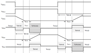
Figure 12 - TDRIVE diagram in DRV834x-Q1 devices.
For example, in the DRV8343H-Q1, the TDRIVE is defaulted to 3000ns, and the VGS falling/rising threshold is around 2V to determine whether a MOSFET is “on” or “off” from the perspective of the DRV8343H-Q1. At t = 0ns, if INHx and INLx inputs are switching, then at t = 3000ns, the gate driver outputs GHx and GLx (with respect to their source voltages) should be at their correct states. If they are not at the correct states, all of the gate driver outputs are disabled and the nFAULT pin will go low.
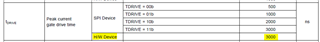
Figure 13 - TDRIVE time defaulted in DRV834x-Q1 hardware devices.
Generally, gate driver faults can occur from a few scenarios:
- The selected IDRIVE or TDRIVE settings are too low to slew the external MOSFET in the desired time. Increasing either the IDRIVE or TDRIVE setting can resolve gate driver faults in these cases.
- If a gate-to-source short occurs on the external MOSFET, a gate driver fault is reported because of the MOSFET gate not turning on.
- There is too much external pulldown resistance (usually less than 10kohm) between the gate and source causing the gate to not turn on sufficiently.
- The gate drive trace widths in the layout are not wide enough (recommended 15-20mil) to support larger IDRIVE values.
- There is internal damage between the driver’s gate and source pins
To determine if a gate driver fault is occurring in hardware devices, measure the following waveforms:
- High-side gate drive outputs: INHx, GHx, SHx, nFAULT
- Low-side gate drive outputs: INLx, GLx, SLx/SPx, nFAULT
If nFAULT goes low after the TDRIVE period from when the INHx or INLx input changes, then it is indicative that a gate drive fault is occurring after the TDRIVE period. Double check by measuring the differential voltage between GHx-SHx and GLx-SLx/SPx to determine if the MOSFET’s VGS voltage is at the correct state.
Thermal Warning/Shutdown (OTW/OTSD)
Overtemperature warning and shutdown occur if the junction temperature of the device exceeds the overtemperature warning or shutdown threshold and hysteresis. If nFAULT spontaneously goes low and recovers, this could be indicative of overtemperature.
This can occur if the PCB layout is insufficient, gate driver settings are too high, or the charge pump or internal regulators are overstressed. This will result in nFAULT automatically latching low until the event is cleared.
Summary of Debug Strategy for Hardware Devices
The following table shows the types of faults that can occur commonly in hardware devices, the timing for those faults, threshold for fault detection, generic recovery method, and waveforms for further debug by triggering on the nFAULT falling edge to determine the fault. Note that waveforms are best captured using low-capacitance probes and/or differential probes measured as close to the DRV as possible due to sensitive circuits affected by parasitics.
|
Fault |
Timing |
Threshold |
Recovery |
Waveforms for further debug (trigger on nFAULT falling edge) |
|
Supply undervoltage |
VM/PVDD UVLO deglitch |
VM/PVDD UVLO falling |
VM/PVDD UVLO rising |
VM/PVDD, nFAULT (zoomed to 10us/div) |
|
Charge pump undervoltage |
CPUV deglitch |
CPUV falling |
CPUV rising |
VCP/CP, VM/PVDD, nFAULT (zoomed to 10us/div) |
|
Gate driver undervoltage |
GVDD/VGLS UVLO deglitch |
GVDD/VGLS falling |
GVDD/VGLS rising |
GVDD/VGLS, nFAULT (zoomed to 10us/div) |
|
Buck undervoltage |
Buck undervoltage deglitch |
VBK_UV falling |
VBK_UV rising |
FB/FB_BK, nFAULT (zoomed to 10us/div) |
|
AVDD/DVDD undervoltage |
AVDD/DVDD UVLO deglitch |
AVDD/DVDD falling |
AVDD/DVDD rising |
FB/FB_BK, nFAULT (zoomed to 10us/div) |
|
VDS overcurrent |
Overcurrent deglitch tOCP_DEG (default value) |
VVDS_OCP (set by VDS pin) |
tRETRY (default value) if input is low |
For HS FET: · INHx, VDRAIN/PVDD, SHx, nFAULT (using four single-ended probes measuring as close as possible to DRV) · INHx, VDRAIN/PVDD-SHx, nFAULT (using two single-ended probes and a differential probe for VDRAIN/PVDD-SHx measuring as close as possible to the DRV) · For automatic retry, zoom to 1ms/div. For cycle-by-cycle current limit, zoom to 20us/div
For LS FET: · INLx, SHx, SLx/SPx, nFAULT (using four single-ended probes measuring as close as possible to DRV) · INHx, SHx-SLx/SPx nFAULT (using two single-ended probes and a differential probe for VDRAIN/PVDD-SHx measuring as close as possible to the DRV) · For automatic retry, zoom to 1ms/div. For cycle-by-cycle current limit, zoom to 20us/div |
|
Next PWM period (1/fPWM) if input rising edge occurs |
||||
|
VSEN overcurrent |
Overcurrent deglitch tOCP_DEG (default value) |
VSEN_OCP (default value) |
tRETRY (default value) |
· INLx, SPx, SNx nFAULT (using four single-ended probes measuring as close as possible to DRV) · INHx, SPx-SNx, nFAULT (using two single-ended probes and a differential probe for VDRAIN/PVDD-SHx measuring as close as possible to the DRV) · Zoom to 1ms/div
|
|
Gate Driver Fault |
TDRIVE (default value) |
~2V |
~2V |
For HS FET: · INHx, GHx, SHx, nFAULT (using single-ended probes measuring as close as possible to DRV) · INHx, GHx-SHx, nFAULT (using two single-ended probes and a differential probe for GHx-SHx measuring as close as possible to the DRV) · Zoom to 1us/div
For LS FET: · INLx, GLx, SPx/SLx, nFAULT (using four single-ended probes measuring as close as possible to DRV) · INLx, GLx-SLx/SPx, nFAULT (using two single-ended probes and a differential probe for GLx-SLx/SPx measuring as close as possible to the DRV) · Zoom to 1us/div |
|
Thermal warning/shutdown |
Automatic (no deglitch) |
TJ > TOTW (warning), TJ > TOTSD (shutdown) |
TJ < TOTW -THYS (warning), TJ > TOTSD -THYS (shutdown) |
VCP/VCPH/CP, GVDD/VGLS, GHx, GLx, nFAULT. Look for any “higher than usual” voltages on gate drive outputs or regulators to indicate overstressing or higher power losses internally. |
