Part Number: DRV8323R
Other Parts Discussed in Thread: ALLIGATOR
Hi,
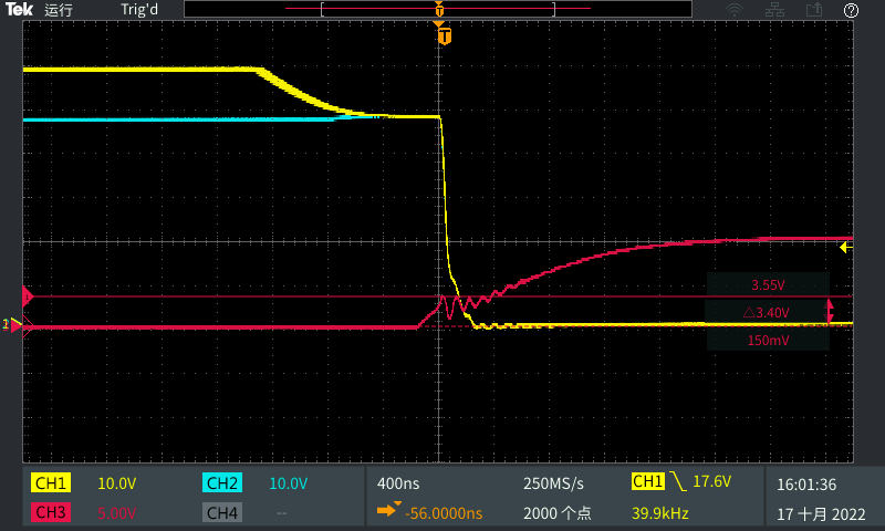
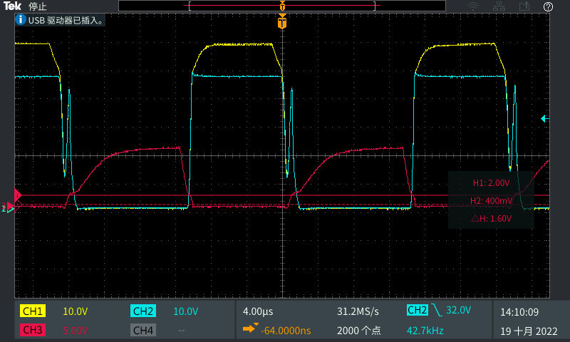
I use DRV8323RS to drive PMSM, but the MOSFETs are burned out at high current or VDS_OCP is indicated.
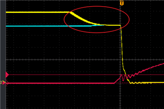
I think it's ringing problem and it seems that the DEAD_TIME does not work during the falling of CHB.
Can you help me check the following waveform and are there ways to improve?
VM: 48V
IDRIVEP_HS: 60mA
IDRIVEN_HS: 120mA
IDRIVEP_LS: 30mA
IDRIVEN_LS: 120mA
DEAD_TIME: 400ns
MOSFET: TPH3R70APL
RED: GLB, YELLOW: GHB, BLUE: SHB