This thread has been locked.

If you have a related question, please click the "Ask a related question" button in the top right corner. The newly created question will be automatically linked to this question.

DRV8323: register value

Part Number: DRV8323

Hi team,

Regarding the original post, the customer still have some motor driver issues may need your help:

The source code for the drive configuration for the 8323 in the SDK is the same as the customer's configuration and the data is not misaligned. 

1) How to confirm that the data was actually written? According to the logic analyzer, 02 and 03 registers are written with return values. Whether write or read, 03 registers return values, but are not the same as written.
A write of the 02 register returns the value written by the customer but does not read any data.

Reads and writes of the 04-06 registers do not return a value, so the customer suspects that they did not write at all. However, from the output, the output value of the chip is changed after writing, enable pin is pulled high and CS has also done a corresponding action.

Does the register lock in register 03 have an effect on read and write? Or are there any pins in hardware that control SPI? 

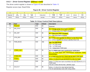
2) Assuming written is good and the customer wants to configure 1X mode (and automatically sensed by Hall), how to configure register values?

Now the value written to register 02 is 1052. However, from the actual hardware tests, the output is not the same as the truth table given in the data manual and the com bit does not seem to be written. 

Could you help check this case? Thanks.

Best Regards,

Cherry

  • Hey Cherry,

    Thank you for your question. I have assigned the thread to a team member and we will aim to provide you a response shortly.


    Best Regards,

    Akshay

  • Hi Cherry,

    For question 1.) could the customer provide a picture of the results of the logic analyzer during a read command and then during a write command to register 04? 

    The register lock in register 03 will lock the ability to write to almost all of the registers if 110b is written to the lock bits. 

    For question 2.) if the customer wrote 1052 to register 02 this corresponds to 0100 0001 1100 in binary which would mean that the COAST bit would be set to 1 (all MOSFETS in Hi-Z state), 1PWM_DIR would be set high, the 1PWM_COM would be set to asynchronous rectification, and the PWM MODE would be set to 6xPWM mode (not 1xPWM mode) Additionally, the customer would be writing a 1 to the reserved bit of register 0x02. I have shown the register settings that the customer is using in yellow below. 


    The main setting that is needed for putting the device into 3xPWM mode is to write 10b to the PWM_MODE bits at address 0x02. I would recommend the customer start with writing 0x080 (decimal 128) to register 02 to set the device in 3xPWM mode. 

    Regards,

    Anthony Lodi