It's the second time when this failure is happening, but this time hopefully we can provide more information.
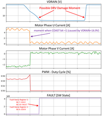
DRV Damage Effect: Gate-Source short is present on DRV output pins GLC(pin18)-to-SPC(pin19) ~4 ohms. MOS-FETs are not affected by the DRV damage.
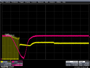
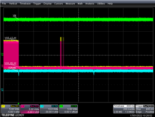
Test Condition: VM = 15V during the test. VDRAIN drops from 25V to 0V. Motor Phase Currents with 0RPM / PH_U=+5A / PH_V=-2.5A / PH_W=-2.5A.
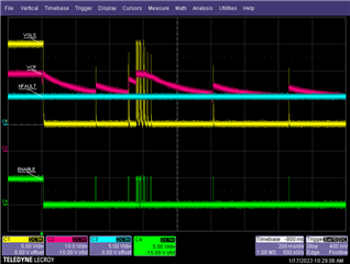
When VDRAIN reaches 17V, COAST bit is set = 1 to force the FETs in Hi-Z, since this is the threshold level of Lower Operating Motor Range.
1.Could this COST=1 request create permanent damages on internal Charge Pump having VDRAIN dropping to 0V?
2.Just after COST=1 request, the input PWMs are set to 50%. Can you confirm that COST bit overwrites the PWM requests and this can't lead to an Charge Pump damage?
3. In case ENABLE is toggled low, having PWM inputs set to 50%. Could this active PWM present during twake lead to a permanent damage of the internal Charge Pumps.