


Other Parts Discussed in Thread: CSD19532Q5B
Hello,
I'm currently designing a product based on the DRV8300 IC. I want to make sure the design is correct in terms of the gate resistors and the MOSFET switching times. Our gate setup is similar to the one presented below:
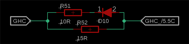
so a separate path for the gate discharge through a diode and a single resistor for charging the gate.
Our FET gate charge:
Total gate charge (10V) 68nC (typical 52nC)
Gate drain charge 8.2nC
The specs are similar to the CSD19532Q5B mentioned in the DRV8300 datasheets. What worries me is that the open/close times of our FETs vary a lot compared to the ones mentioned in the datasheet with a very similar setup. In result we have to apply much bigger gate resistors to achieve correct times (around 100ns) and mitigate overshoots.
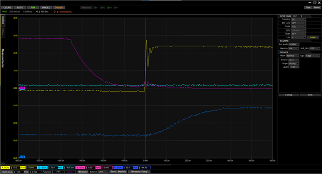
Probes setup:
CH1 - phase voltage (LS D-S voltage)
CH2 - N/A
CH3 - G-S LS voltage
CH4 - current sense after amplifier (note: the amplifier BW is too little to show high speed changes in the phase current, thus only current direction should be considered. The measurement was made with a solder-in diy probe so the voltage scale is not correct)
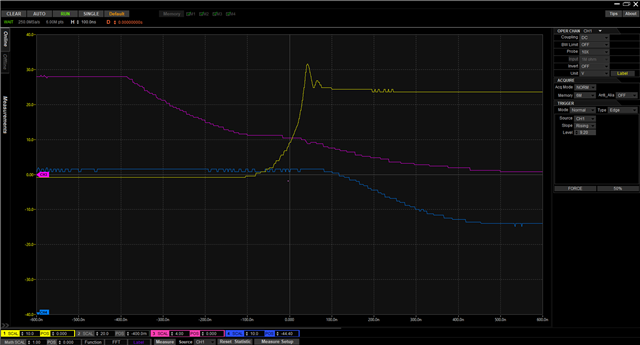
We observed two types of ringing due to parasitic inductances happening when the mosfets open and close while the maximum current is flowing through the phase in either direction.
Both pictures with 27R in the gate charge path and 10R in gate discharge path on both HS and LS:
positive current (40A):
negative current (-40A):
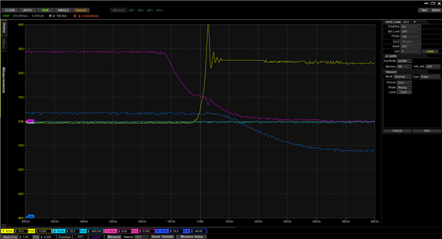
As can be seen the overshoots are quire severe and they occur when high side FET opens too fast (picture #1) and when low side closes too fast (picture #2).
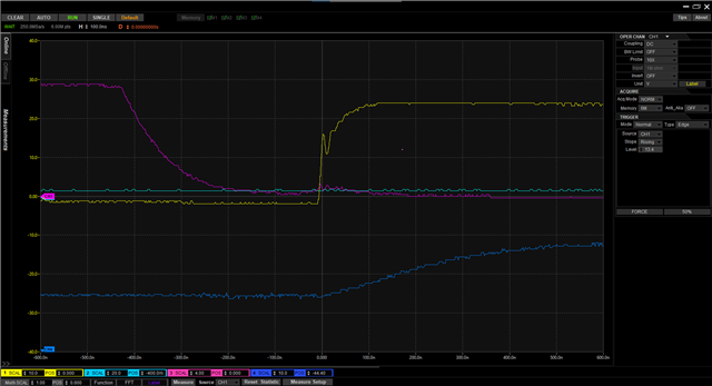
The first scenario was easy to fix, since increasing the gate charge resistor form 27R to 60R fixed the overshoots almost completely:
The second scenario was rather harder to solve since it turned out that discharge resistor must be larger than the charge resistor (so the diode had to be placed in reverse). This is the result when the charge resistor is 20R and discharge is 47R. In this scenario a partial cross conduction occurs so the dead time should be made larger (current is around 235ns).
I just wanted to make sure these large resistor values are correct (compared to the reference design form the datasheet).
Best Regards,
Piotr Wasilewski
